SLVSA30D April 2011 – March 2019 UCD9090
PRODUCTION DATA.
- 1 Features
- 2 Applications
- 3 Description
- 4 Revision History
- 5 Pin Configuration and Functions
- 6 Specifications
-
7 Detailed Description
- 7.1 Overview
- 7.2 Functional Block Diagram
- 7.3 Feature Description
- 7.4
Device Functional Modes
- 7.4.1 Power-Supply Sequencing
- 7.4.2 Pin-Selected Rail States
- 7.4.3 Monitoring
- 7.4.4 Fault Responses and Alert Processing
- 7.4.5 Shut Down All Rails and Sequence On (Resequence)
- 7.4.6 GPIOs
- 7.4.7 GPO Control
- 7.4.8 GPO Dependencies
- 7.4.9 GPI Special Functions
- 7.4.10 Power-Supply Enable Pins
- 7.4.11 Cascading Multiple Devices
- 7.4.12 PWM Outputs
- 7.4.13 Programmable Multiphase PWMs
- 7.4.14 Margining
- 7.4.15 Run Time Clock
- 7.4.16 System Reset Signal
- 7.4.17 Watch Dog Timer
- 7.4.18 Data and Error Logging to Flash Memory
- 7.4.19 Brownout Function
- 7.4.20 PMBus Address Selection
- 7.4.21 Device Reset
- 7.4.22 JTAG Interface
- 7.4.23 Internal Fault Management and Memory Error Correction (ECC)
- 7.5 Programming
- 8 Application and Implementation
- 9 Power Supply Recommendations
- 10Layout
- 11Device and Documentation Support
- 12Mechanical, Packaging, and Orderable Information
Package Options
Mechanical Data (Package|Pins)
- RGZ|48
Thermal pad, mechanical data (Package|Pins)
- RGZ|48
Orderable Information
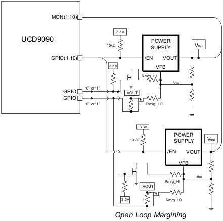
7.4.14.1 Open-Loop Margining
Open-loop margining is done by connecting a power-supply feedback node to ground through one resistor and to the margined power supply output (VOUT) through another resistor. The power-supply regulation loop responds to the change in feedback node voltage by increasing or decreasing the power-supply output voltage to return the feedback voltage to the original value. The voltage change is determined by the fixed resistor values and the voltage at VOUT and ground. Two GPIO pins must be configured as open-drain outputs for connecting resistors from the feedback node of each power supply to VOUT or ground.
 Figure 23. Open-Loop Margining