SBOS395D October 2007 – September 2015 VCA820
PRODUCTION DATA.
- 1 Features
- 2 Applications
- 3 Description
- 4 Revision History
- 5 Device Options
- 6 Pin Configuration and Functions
-
7 Specifications
- 7.1 Absolute Maximum Ratings
- 7.2 ESD Ratings
- 7.3 Recommended Operating Conditions
- 7.4 Thermal Information
- 7.5 Electrical Characteristics: VS = ±5 V
- 7.6 Typical Characteristics: VS = ±5 V, DC Parameters
- 7.7 Typical Characteristics: VS = ±5 V, DC and Power-Supply Parameters
- 7.8 Typical Characteristics: VS = ±5 V, AVMAX = 6 dB
- 7.9 Typical Characteristics: VS = ±5 V, AVMAX = 20 dB
- 7.10 Typical Characteristics: VS = ±5 V, AVMAX = 40 dB
- 8 Detailed Description
- 9 Application and Implementation
- 10Power Supply Recommendations
- 11Layout
- 12Device and Documentation Support
- 13Mechanical, Packaging, and Orderable Information
Package Options
Mechanical Data (Package|Pins)
Thermal pad, mechanical data (Package|Pins)
Orderable Information
1 Features
2 Applications
- AGC Receivers With RSSI
- Differential Line Receivers
- Pulse Amplitude Compensation
- Variable Attenuators
3 Description
The VCA820 is a dc-coupled, wideband, linear in dB, continuously variable, voltage-controlled gain amplifier. The VCA820 provides a differential input to single-ended conversion with a high-impedance gain control input, used to vary the gain down 40 dB from the nominal maximum gain set by the gain resistor (RG) and feedback resistor (RF).
The VCA820 internal architecture consists of two input buffers and an output current feedback amplifier stage, integrated with a multiplier core to provide a complete variable gain amplifier (VGA) system that does not require external buffering. The maximum gain is set externally with two resistors, providing flexibility in designs. The maximum gain is intended to be set between +2 V/V and +100 V/V. Operating from ±5-V supplies, the gain control voltage for the VCA820 adjusts the gain linearly in dB as the control voltage varies from 0 V to +2 V. For example, set for a maximum gain of +10 V/V, the VCA820 provides 20 dB, at +2-V input, to –20 dB at 0-V input of gain control range. The VCA820 offers excellent gain linearity. For a 20-dB maximum gain, and a gain-control input voltage varying between 1 V and 2 V, the gain does not deviate by more than ±0.4dB (maximum at +25°C).
Device Information(1)
| PART NUMBER | PACKAGE | BODY SIZE (NOM) |
|---|---|---|
| VCA820 | SOIC (14) | 8.65 mm × 3.91 mm |
| VSSOP (10) | 3.00 mm × 3.00 mm |
- For all available packages, see the orderable addendum at the end of the data sheet.
space
space
space
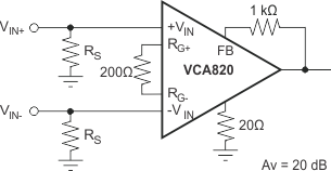
Wideband Differential to Single-Ended Amplifier

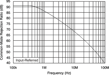
Common-Mode Rejection Ratio
