SBOS913 February 2018 XTR305
PRODUCTION DATA.
- 1 Features
- 2 Applications
- 3 Description
- 4 Revision History
- 5 Pin Configuration and Functions
-
6 Specifications
- 6.1 Absolute Maximum Ratings
- 6.2 ESD Ratings
- 6.3 Recommended Operating Conditions
- 6.4 Thermal Information
- 6.5 Electrical Characteristics: Voltage Output Mode
- 6.6 Electrical Characteristics: Current Output Mode
- 6.7 Electrical Characteristics: Operational Amplifier (OPA)
- 6.8 Electrical Characteristics: Instrumentation Amplifier (IA)
- 6.9 Electrical Characteristics: Current Monitor
- 6.10 Electrical Characteristics: Power and Digital
- 6.11 Typical Characteristics
- 7 Detailed Description
-
8 Application and Implementation
- 8.1 Application Information
- 8.2
Typical Application
- 8.2.1 Design Requirements
- 8.2.2
Detailed Design Procedure
- 8.2.2.1 Voltage Output Mode
- 8.2.2.2 Current Output Mode
- 8.2.2.3 Input Signal Connection
- 8.2.2.4 Externally-Configured Mode: OPA and IA
- 8.2.2.5 Driver Output Disable
- 8.2.2.6 Driving Capacitive Loads and Loop Compensation
- 8.2.2.7 Internal Current Sources, Switching Noise, and Settling Time
- 8.2.2.8 IA Structure, Voltage Monitor
- 8.2.2.9 Digital I/O and Ground Considerations
- 8.2.2.10 Output Protection
- 8.2.3 Application Curves
- 9 Power Supply Recommendations
- 10Layout
- 11Device and Documentation Support
- 12Mechanical, Packaging, and Orderable Information
Package Options
Mechanical Data (Package|Pins)
- RGW|20
Thermal pad, mechanical data (Package|Pins)
- RGW|20
Orderable Information
8.2.2.1 Voltage Output Mode
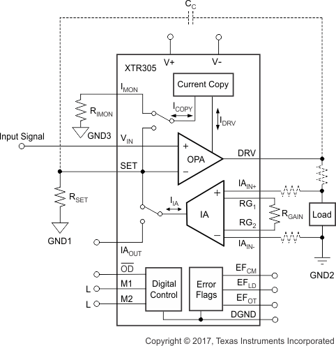
In voltage output mode (M1 and M2 are connected low or left unconnected), the feedback loop through the IA provides high impedance remote sensing of the voltage at the destination, compensating the resistance of a protection circuit, switches, wiring, and connector resistance. The output of the IA is a current that is proportional to the input voltage. This current is internally routed to the OPA summing junction through a multiplexer, as shown in Figure 41.
A 1:10 copy of the output current of the OPA can be monitored at the IMON pin. This output current and the known output voltage can be used to calculate the load resistance or load power.
During an output short-circuit or an overcurrent condition the XTR305 output current is limited and EFLD (load error, active low) flag is activated.
 Figure 41. Simplified Voltage Output Mode Configuration
Applications not requiring the remote sense feature can use the OPA in stand-alone operation (M1 = high). In this case, the IA is available as a separate input channel.
The IA gain can be set by two resistors, RGAIN and RSET (Equation 1):

or when adding an offset, VREF, to get bidirectional output with a single-ended input shown in Equation 2:

The RSET resistor is also used in current output mode. Therefore, it is useful to define RSET for the current mode, then set the ratio between current and voltage span with RGAIN.