SBAS689D June 2015 – December 2016 AFE4404
PRODUCTION DATA.
- 1 Features
- 2 Applications
- 3 Description
- 4 Revision History
- 5 Device Comparison Table
- 6 Pin Configuration and Functions
- 7 Specifications
-
8 Detailed Description
- 8.1 Overview
- 8.2 Functional Block Diagram
- 8.3 Feature Description
- 8.4 Device Functional Modes
- 8.5
Register Map
- 8.5.1 Register 0h (address = 0h) [reset = 0h]
- 8.5.2 Register 1h (address = 1h) [reset = 0h]
- 8.5.3 Register 2h (address = 2h) [reset = 0h]
- 8.5.4 Register 3h (address = 3h) [reset = 0h]
- 8.5.5 Register 4h (address = 4h) [reset = 0h]
- 8.5.6 Register 5h (address = 5h) [reset = 0h]
- 8.5.7 Register 6h (address = 6h) [reset = 0h]
- 8.5.8 Register 7h (address = 7h) [reset = 0h]
- 8.5.9 Register 8h (address = 8h) [reset = 0h]
- 8.5.10 Register 9h (address = 9h) [reset = 0h]
- 8.5.11 Register Ah (address = Ah) [reset = 0h]
- 8.5.12 Register Bh (address = Bh) [reset = 0h]
- 8.5.13 Register Ch (address = Ch) [reset = 0h]
- 8.5.14 Register Dh (address = Dh) [reset = 0h]
- 8.5.15 Register Eh (address = Eh) [reset = 0h]
- 8.5.16 Register Fh (address = Fh) [reset = 0h]
- 8.5.17 Register 10h (address = 10h) [reset = 0h]
- 8.5.18 Register 11h (address = 11h) [reset = 0h]
- 8.5.19 Register 12h (address = 12h) [reset = 0h]
- 8.5.20 Register 13h (address = 13h) [reset = 0h]
- 8.5.21 Register 14h (address = 14h) [reset = 0h]
- 8.5.22 Register 15h (address = 15h) [reset = 0h]
- 8.5.23 Register 16h (address = 16h) [reset = 0h]
- 8.5.24 Register 17h (address = 17h) [reset = 0h]
- 8.5.25 Register 18h (address = 18h) [reset = 0h]
- 8.5.26 Register 19h (address = 19h) [reset = 0h]
- 8.5.27 Register 1Ah (address = 1Ah) [reset = 0h]
- 8.5.28 Register 1Bh (address = 1Bh) [reset = 0h]
- 8.5.29 Register 1Ch (address = 1Ch) [reset = 0h]
- 8.5.30 Register 1Dh (address = 1Dh) [reset = 0h]
- 8.5.31 Register 1Eh (address = 1Eh) [reset = 0h]
- 8.5.32 Register 20h (address = 20h) [reset = 0h]
- 8.5.33 Register 21h (address = 21h) [reset = 0h]
- 8.5.34 Register 22h (address = 22h) [reset = 0h]
- 8.5.35 Register 23h (address = 23h) [reset = 0h]
- 8.5.36 Register 29h (address = 29h) [reset = 0h]
- 8.5.37 Register 2Ah (address = 2Ah) [reset = 0h]
- 8.5.38 Register 2Bh (address = 2Bh) [reset = 0h]
- 8.5.39 Register 2Ch (address = 2Ch) [reset = 0h]
- 8.5.40 Register 2Dh (address = 2Dh) [reset = 0h]
- 8.5.41 Register 2Eh (address = 2Eh) [reset = 0h]
- 8.5.42 Register 2Fh (address = 2Fh) [reset = 0h]
- 8.5.43 Register 31h (address = 31h) [reset = 0h]
- 8.5.44 Register 32h (address = 32h) [reset = 0h]
- 8.5.45 Register 33h (address = 33h) [reset = 0h]
- 8.5.46 Register 34h (address = 34h) [reset = 0h]
- 8.5.47 Register 35h (address = 35h) [reset = 0h]
- 8.5.48 Register 36h (address = 36h) [reset = 0h]
- 8.5.49 Register 37h (address = 37h) [reset = 0h]
- 8.5.50 Register 39h (address = 39h) [reset = 0h]
- 8.5.51 Register 3Ah (address = 3Ah) [reset = 0h]
- 8.5.52 Register 3Dh (address = 3Dh) [reset = 0h]
- 8.5.53 Register 3Fh (address = 3Fh) [reset = 0h]
- 8.5.54 Register 40h (address = 40h) [reset = 0h]
- 9 Application and Implementation
- 10Power Supply Recommendations
- 11Layout
- 12Device and Documentation Support
- 13Mechanical, Packaging, and Orderable Information
Package Options
Refer to the PDF data sheet for device specific package drawings
Mechanical Data (Package|Pins)
- YZP|15
Thermal pad, mechanical data (Package|Pins)
Orderable Information
1 Features
- Transmitter:
- Supports Common Anode LED Configuration
- Dynamic Range: 100 dB
- 6-Bit Programmable LED Current to 50 mA (Extendable to 100 mA)
- Programmable LED On-Time
- Simultaneous Support of 3 LEDs for Optimized SpO2, HRM, or Multi-Wavelength HRM
- Receiver:
- 24-Bit Representation of the Current Input from a Photodiode in Twos Complement Format
- Individual DC Offset Subtraction DAC at TIA Input for Each LED and Ambient Phase
- Digital Ambient Subtraction at ADC Output
- Programmable Transimpedance Gain:
10 kΩ to 2 MΩ - Dynamic Range: 100 dB
- Average Current Less Than 200 μA for PPG Signal Acquisition
- Pulse Frequency: 10 SPS to 1000 SPS
- Flexible Pulse Sequencing and Timing Control
- Flexible Clock Options:
- External Clocking:
4-MHz to 60-MHz Input Clock - Internal Clocking: 4-MHz Oscillator
- External Clocking:
- I2C Interface
- Operating Temperature Range: –20°C to 70°C
- 2.6-mm × 1.6-mm DSBGA Package, 0.5-mm Pitch
- Supplies: Rx: 2 V to 3.6 V, Tx: 3 V to 5.25 V,
IO: 1.8 V to 3.6 V
2 Applications
- Optical Heart-Rate Monitoring (HRM)
- Heart-Rate Variability (HRV)
- Pulse Oximetry (SpO2 Measurement)
- VO2 Max
- Calorie Expenditure
3 Description
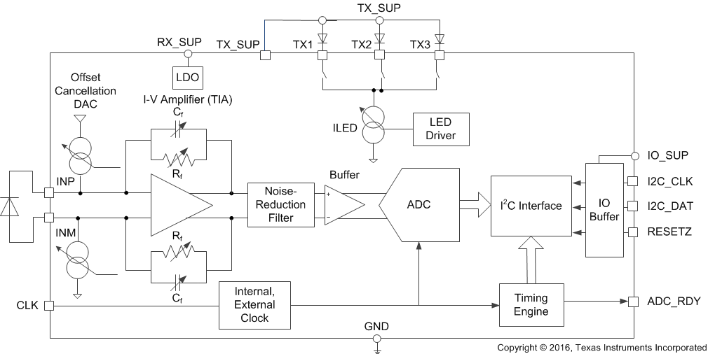
The AFE4404 is an analog front-end (AFE) for optical bio-sensing applications, such as heart-rate monitoring (HRM) and saturation of peripheral capillary oxygen (SpO2). The device supports three switching light-emitting diodes (LEDs) and a single photodiode. The current from the photodiode is converted into voltage by the transimpedance amplifier (TIA) and digitized using an analog-to-digital converter (ADC). The ADC code can be read out using an I2C interface. The AFE also has a fully-integrated LED driver with a 6-bit current control. The device has a high dynamic range transmit and receive circuitry that helps with the sensing of very small signal levels.
- For all available packages, see the orderable addendum at the end of the datasheet.
- Refers to dimensions D × E in Figure 99.
Simplified Block Diagram
