SBOS539A December 2010 – April 2016 INA203-Q1
PRODUCTION DATA.
- 1 Features
- 2 Applications
- 3 Description
- 4 Revision History
- 5 Device Comparison Table
- 6 Pin Configuration and Functions
-
7 Specifications
- 7.1 Absolute Maximum Ratings
- 7.2 ESD Ratings
- 7.3 Recommended Operating Conditions
- 7.4 Thermal Information
- 7.5 Electrical Characteristics: Current-Shunt Monitor
- 7.6 Electrical Characteristics: Comparator
- 7.7 Electrical Characteristics: Reference
- 7.8 Electrical Characteristics: General
- 7.9 Typical Characteristics
- 8 Detailed Description
- 9 Application and Implementation
- 10Power Supply Recommendations
- 11Layout
- 12Device and Documentation Support
- 13Mechanical, Packaging, and Orderable Information
Package Options
Mechanical Data (Package|Pins)
- PW|14
Thermal pad, mechanical data (Package|Pins)
Orderable Information
1 Features
- Qualified for Automotive Applications
- Current Sense Amplifier
- Common-Mode Range: –16 V to +80 V
- Accuracy: 3.5% (Maximum) Over Temperature
- Bandwidth: 500 kHz
- Gain: 20 V/V
- Integrated Dual Comparators:
- Comparator 1 With Latch
- Comparator 2 With Optional Delay
- Quiescent Current: 1.8 mA
- Latch-Up Performance Meets 100 mA Per AEC-Q100, Level I
- Packages: TSSOP-14
2 Applications
3 Description
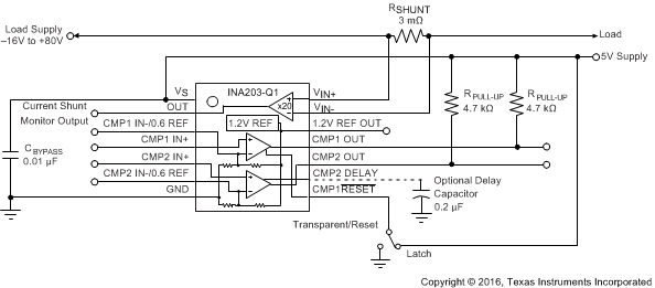
The INA203-Q1 is a unidirectional current-shunt monitor (also called a current sense amplifier) with voltage output, dual comparators, and voltage reference. The INA203-Q1 can sense drops across shunts at common-mode voltages from –16 V to +80 V. The INA203-Q1 is available with 20-V/V gain with up to 500-kHz bandwidth.
The INA203-Q1 incorporates two open-drain comparators with internal 0.6-V references and also provides a 1.2-V reference output. The comparator references can be overridden by external inputs. Comparator 1 includes a latching capability, and Comparator 2 has a user-programmable delay.
The INA203-Q1 operates from a single 2.7 V to 18 V supply. It is specified over the extended operating temperature range of –40°C to +125°C.
Device Information(1)
| PART NUMBER | PACKAGE | BODY SIZE (NOM) |
|---|---|---|
| INA203-Q1 | TSSOP (14) | 5.00 mm × 4.40 mm |
- For all available packages, see the orderable addendum at the end of the data sheet.
