SNAS466G February 2009 – December 2016 ADC10D1000QML-SP
PRODUCTION DATA.
- 1 Features
- 2 Applications
- 3 Description
- 4 Revision History
- 5 Pin Configuration and Functions
-
6 Specifications
- 6.1 Absolute Maximum Ratings
- 6.2 ESD Ratings
- 6.3 Recommended Operating Conditions
- 6.4 Thermal Information
- 6.5 Converter Electrical Characteristics: Static Converter Characteristics
- 6.6 Converter Electrical Characteristics: Dynamic Converter Characteristics
- 6.7 Converter Electrical Characteristics: Analog Input/Output and Reference Characteristics
- 6.8 Converter Electrical Characteristics: Channel-to-Channel Characteristics
- 6.9 Converter Electrical Characteristics: LVDS CLK Input Characteristics
- 6.10 Electrical Characteristics: AutoSync Feature
- 6.11 Converter Electrical Characteristics: Digital Control and Output Pin Characteristics
- 6.12 Converter Electrical Characteristics: Power Supply Characteristics (1:2 Demux Mode)
- 6.13 Converter Electrical Characteristics: AC Electrical Characteristics
- 6.14 Timing Requirements: Serial Port Interface
- 6.15 Timing Requirements: Calibration
- 6.16 Quality Conformance Inspection
- 6.17 Timing Diagrams
- 6.18 Typical Characteristics
-
7 Detailed Description
- 7.1 Overview
- 7.2 Functional Block Diagram
- 7.3 Feature Description
- 7.4
Device Functional Modes
- 7.4.1
Control Modes
- 7.4.1.1
Non-Extended Control Mode
- 7.4.1.1.1 Non-Demultiplexed Mode Pin (NDM)
- 7.4.1.1.2 Dual Data-Rate Phase Pin (DDRPh)
- 7.4.1.1.3 Calibration Pin (CAL)
- 7.4.1.1.4 Power-Down I-Channel Pin (PDI)
- 7.4.1.1.5 Power-Down Q-Channel Pin (PDQ)
- 7.4.1.1.6 Test Pattern Mode Pin (TPM)
- 7.4.1.1.7 Full-Scale Input Range Pin (FSR)
- 7.4.1.1.8 AC-DC-Coupled Mode Pin (VCMO)
- 7.4.1.1.9 LVDS Output Common-Mode Pin (VBG)
- 7.4.1.1
Non-Extended Control Mode
- 7.4.2 Extended Control Mode
- 7.4.1
Control Modes
- 7.5 Programming
- 7.6 Register Maps
- 8 Application and Implementation
- 9 Power Supply Recommendations
- 10Layout
- 11Device and Documentation Support
- 12Mechanical, Packaging, and Orderable Information
パッケージ・オプション
デバイスごとのパッケージ図は、PDF版データシートをご参照ください。
メカニカル・データ(パッケージ|ピン)
- NAA|376
サーマルパッド・メカニカル・データ
発注情報
9 Power Supply Recommendations
9.1 Power Planes
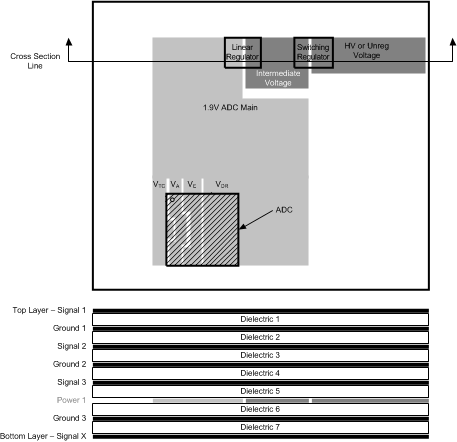
Source all supply buses for the ADC from a common linear voltage regulator. This ensures that all power buses to the ADC are turned on and off simultaneously. This single source is split into individual sections of the power plane, with individual decoupling and connection to the different power supply buses of the ADC. Due to the low voltage but relatively high supply current requirement, the optimal solution may be to use a switching regulator to provide an intermediate low voltage, which is then regulated down to the final ADC supply voltage by a linear regulator. Refer to the documentation provided for the ADC10D1000RB for additional details on specific regulators that TI recommends for this configuration.
Provide power for the ADC through a broad plane, which is located on one layer adjacent to the ground plane(s). Placing the power and ground planes on adjacent layers provides low impedance decoupling of the ADC supplies, especially at higher frequencies. The output of a linear regulator must feed into the power plane through a low impedance multi-via connection. Split the power plane into individual power peninsulas near the ADC. Each peninsula should feed a particular power bus on the ADC, with decoupling for that power bus connecting the peninsula to the ground plane near each power/ground pin pair. Using this technique can be difficult on many printed circuit CAD tools. To work around this, 0-Ω resistors can be used to connect the power source net to the individual nets for the different ADC power buses. As a final step, the 0-Ω resistors can be removed, and the plane and peninsulas can be connected manually after all other error checking is completed.
9.1.1 Bypass Capacitors
The general recommendation is to have one 100-nF capacitor for each power/ground pin pair. The capacitors must be surface mount multi-layer ceramic chip capacitors similar to Presidio SR0402X7R104KENG5.
9.1.1.1 Ground Plane
Grounding must be done using continuous full ground planes to minimize the impedance for all ground return paths, and provide the shortest possible image/return path for all signal traces.
9.1.1.2 Power Supply Example
The ADC10D1000RB uses continuous ground planes (except where clear areas are needed to provide appropriate impedance management for specific signals), see Figure 49. Power is provided on one plane, with the 1.9-V ADC supply being split into multiple zones or peninsulas for the specific power buses of the ADC. Decoupling capacitors are connected between these power bus peninsulas and the adjacent power planes using vias. The capacitors are located as close to the individual power/ground pin pairs of the ADC as possible. In most cases, this means the capacitors are located on the opposite side of the PCB to the ADC.
 Figure 49. Power and Grounding Example