JAJSLJ3A December 2021 – April 2022 ADC128S102-SEP
PRODUCTION DATA
- 1 特長
- 2 アプリケーション
- 3 概要
- 4 Revision History
- 5 Pin Configuration and Functions
- 6 Specifications
- 7 Detailed Description
- 8 Application and Implementation
- 9 Power Supply Recommendations
- 10Layout
- 11Device and Documentation Support
- 12Mechanical, Packaging, and Orderable Information
7.3.2 Analog Inputs
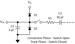
Figure 7-2 shows an equivalent circuit for one of the input channels of the ADC128S102-SEP. Diodes D1 and D2 provide ESD protection for the analog inputs. The operating range for the analog inputs is 0 V to VA. Going beyond this range causes the ESD diodes to conduct and results in erratic operation.
Capacitor C1 in Figure 7-2 has a typical value of 3 pF and is mainly the package pin capacitance. Resistor R1 is the ON-resistance of the multiplexer and track-and-hold switch and is typically 500 Ω. Capacitor C2 is the ADC128S102-SEP sampling capacitor, and is typically 30 pF. The ADC128S102-SEP delivers best performance when driven by a low-impedance source (less than 100 Ω). This source is especially important when using the ADC128S102-SEP to sample dynamic signals. Also important when sampling dynamic signals is a band-pass or low-pass filter, which reduces harmonics and noise in the input. These filters are often referred to as antialiasing filters.
 Figure 7-2 Equivalent Input Circuit