JAJSHP1E July 2014 – June 2022 ADC3221 , ADC3222 , ADC3223 , ADC3224
PRODUCTION DATA
- 1 特長
- 2 アプリケーション
- 3 概要
- 4 Revision History
- 5 Pin Configuration and Functions
-
6 Specifications
- 6.1 Absolute Maximum Ratings
- 6.2 ESD Ratings
- 6.3 Recommended Operating Conditions (1)
- 6.4 Thermal Information
- 6.5 Electrical Characteristics: General
- 6.6 Electrical Characteristics: ADC3221, ADC3222
- 6.7 Electrical Characteristics: ADC3223, ADC3224
- 6.8 AC Performance: ADC3221
- 6.9 AC Performance: ADC3222
- 6.10 AC Performance: ADC3223
- 6.11 AC Performance: ADC3224
- 6.12 Digital Characteristics
- 6.13 Timing Requirements: General
- 6.14 Timing Requirements: LVDS Output
- 6.15 Typical Characteristics: ADC3221
- 6.16 Typical Characteristics: ADC3222
- 6.17 Typical Characteristics: ADC3223
- 6.18 Typical Characteristics: ADC3224
- 6.19 Typical Characteristics: Common
- 6.20 Typical Characteristics: Contour
- 7 Parameter Measurement Information
-
8 Detailed Description
- 8.1 Overview
- 8.2 Functional Block Diagram
- 8.3 Feature Description
- 8.4 Device Functional Modes
- 8.5 Programming
- 8.6
Register Maps
- 8.6.1 Summary of Special Mode Registers
- 8.6.2
Serial Register Description
- 8.6.2.1 Register 01h
- 8.6.2.2 Register 03h
- 8.6.2.3 Register 04h
- 8.6.2.4 Register 05h
- 8.6.2.5 Register 06h
- 8.6.2.6 Register 07h
- 8.6.2.7 Register 09h
- 8.6.2.8 Register 0Ah
- 8.6.2.9 Register 0Bh
- 8.6.2.10 Register 0Eh
- 8.6.2.11 Register 0Fh
- 8.6.2.12 Register 13h
- 8.6.2.13 Register 15h
- 8.6.2.14 Register 25h
- 8.6.2.15 Register 27h
- 8.6.2.16 Register 41Dh
- 8.6.2.17 Register 422h
- 8.6.2.18 Register 434h
- 8.6.2.19 Register 439h
- 8.6.2.20 Register 51Dh
- 8.6.2.21 Register 522h
- 8.6.2.22 Register 534h
- 8.6.2.23 Register 539h
- 8.6.2.24 Register 608h
- 8.6.2.25 Register 70Ah
- 9 Applications and Implementation
- 10Device and Documentation Support
- 11Mechanical, Packaging, and Orderable Information
パッケージ・オプション
メカニカル・データ(パッケージ|ピン)
- RGZ|48
サーマルパッド・メカニカル・データ
- RGZ|48
発注情報
8.5.1.1.2 Serial Register Readout
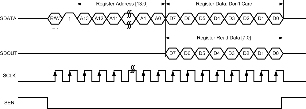
The device includes a mode where the contents of the internal registers can be read back using the SDOUT pin. This readback mode can be useful as a diagnostic check to verify the serial interface communication between the external controller and the ADC. The procedure to read the contents of the serial registers is as follows:
- Drive the SEN pin low.
- Set the R/W bit (A15) to 1. This setting disables any further writes to the registers.
- Set bit A14 in the address field to 1.
- Initiate a serial interface cycle specifying the address of the register (A[13:0]) whose content must be read.
- The device outputs the contents (D[7:0]) of the selected register on the SDOUT pin.
- The external controller can latch the contents at the SCLK rising edge.
- To enable register writes, reset the R/W register bit to 0.
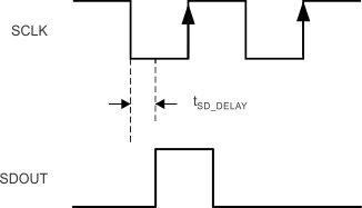
When READOUT is disabled, the SDOUT pin is in a high-impedance mode. If serial readout is not used, the SDOUT pin must float. Figure 8-14 shows a timing diagram of the serial register read operation. Data appear on the SDOUT pin at the SCLK falling edge with an approximate delay (tSD_DELAY) of 20 ns, as shown in Figure 8-15.
 Figure 8-14 Serial Register Read Timing Diagram
 Figure 8-15 SDOUT Timing Diagram