JAJSP40A March 2022 – October 2022 ADS117L11
PRODUCTION DATA
- 1 特長
- 2 アプリケーション
- 3 概要
- 4 Revision History
- 5 Pin Configuration and Functions
-
6 Specifications
- 6.1 Absolute Maximum Ratings
- 6.2 ESD Ratings
- 6.3 Recommended Operating Conditions
- 6.4 Thermal Information
- 6.5 Electrical Characteristics
- 6.6 Timing Requirements (1.65 V ≤ IOVDD ≤ 2 V)
- 6.7 Switching Characteristics (1.65 V ≤ IOVDD ≤ 2 V)
- 6.8 Timing Requirements (2 V < IOVDD ≤ 5.5 V)
- 6.9 Switching Characteristics (2 V < IOVDD ≤ 5.5 V)
- 6.10 Timing Diagrams
- 6.11 Typical Characteristics
- 7 Parameter Measurement Information
-
8 Detailed Description
- 8.1 Overview
- 8.2 Functional Block Diagram
- 8.3 Feature Description
- 8.4 Device Functional Modes
- 8.5 Programming
- 8.6
Registers
- 8.6.1 DEV_ID Register (Address = 0h) [reset = 01h]
- 8.6.2 REV_ID Register (Address = 1h) [reset = xxh]
- 8.6.3 STATUS Register (Address = 2h) [reset = x1100xxxb]
- 8.6.4 CONTROL Register (Address = 3h) [reset = 00h]
- 8.6.5 MUX Register (Address = 4h) [reset = 00h]
- 8.6.6 CONFIG1 Register (Address = 5h) [reset = 00h]
- 8.6.7 CONFIG2 Register (Address = 6h) [reset = 00h]
- 8.6.8 CONFIG3 Register (Address = 7h) [reset = 00h]
- 8.6.9 CONFIG4 Register (Address = 8h) [reset = 08h]
- 8.6.10 OFFSET2, OFFSET1, OFFSET0 Registers (Addresses = 9h, Ah, Bh) [reset = 00h, 00h, 00h]
- 8.6.11 GAIN2, GAIN1, GAIN0 Registers (Addresses = Ch, Dh, Eh) [reset = 40h, 00h, 00h]
- 8.6.12 CRC Register (Address = Fh) [reset = 00h]
- 9 Application and Implementation
- 10Device and Documentation Support
- 11Mechanical, Packaging, and Orderable Information
パッケージ・オプション
デバイスごとのパッケージ図は、PDF版データシートをご参照ください。
メカニカル・データ(パッケージ|ピン)
- RUK|20
サーマルパッド・メカニカル・データ
発注情報
8.3.5.1 Wideband Filter
The wideband filter is a multistage FIR filter design featuring linear phase response, low pass-band ripple, narrow transition band, and high stop-band attenuation. Because of the excellent frequency domain performance, the wideband filter is effective for measuring ac signals. The ADC provides eight programmable oversampling ratios (OSR) and two speed modes, offering a range of data rates, resolution, and device power consumption to select from.
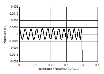
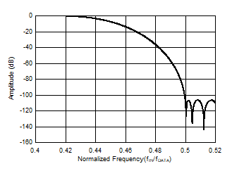
Figure 8-8 through Figure 8-12 illustrate the frequency response of the wideband filter. Figure 8-8 shows the pass-band ripple. Figure 8-9 shows the detailed frequency response at the transition band.
 Figure 8-8 Wideband Filter Pass-Band
Ripple
 Figure 8-9 Wideband Filter Transition
Band
Figure 8-9 Wideband Filter Transition
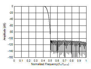
BandFigure 8-10 shows the frequency response to fDATA for OSR ≥ 64. The stop band begins at fDATA / 2 to prevent aliasing at the Nyquist frequency. Figure 8-11 shows the stop-band attenuation to fMOD for OSR = 32. In the stop-band region, out-of-band input frequencies intermodulate with multiples of the chop frequency at fMOD / 32, creating a pattern of response peaks that exceed the stop-band attenuation of the digital filter. The frequency width of each response peak is twice the bandwidth of the filter. Improved stop-band attenuation is provided by using an antialias filter at the ADC input. See the Section 9.2 section for details of a fourth-order antialias filter.

| OSR ≥ 64 |
| OSR = 32 |
Figure 8-12 shows the filter response centered around fMOD. As shown, the filter response repeats at fMOD. If not removed by an antialiasing filter, input frequencies at fMOD appear as aliased frequencies in the pass band. Aliasing also occurs with input frequencies occurring at multiples of fMOD. The aliased frequency bands are defined by:
where:
- N = 1, 2, 3, and so on
- fMOD = Modulator sampling frequency
- fBW = Filter bandwidth
The group delay of the filter is the time for a continuous input signal to propagate from the filter input to the filter output. Because the filter is a linear-phase design, the envelope of a complex input signal is undistorted by the filter. The group delay (expressed in units of time) is constant versus frequency equal to the value = 34 / fDATA. After a step change is applied to the ADC input (when synchronous to DRDY falling edge), fully settled data occurs 68 data periods later. Figure 8-13 illustrates the filter group delay (34 / fDATA) and the settling time of a step input (68 / fDATA).
The digital filter is restarted when the ADC is synchronized. The ADC suppresses the first 68 conversion periods until the filter is fully settled. There is no need to discard data after synchronization. The duration of data suppression is the conversion latency time as listed in the latency time column of Table 8-3. A 0.4-μs fixed overhead time is incurred for all data rates. If a step change input is applied without synchronizing the ADC, then the next 69 conversions are partially settled data.
| OSR | DATA RATE (kSPS) | –0.1-dB FREQUENCY (kHz) | –3-dB FREQUENCY (kHz) | LATENCY TIME (µs)(1) |
|---|---|---|---|---|
| HIGH-SPEED MODE (fCLK = 25.6 MHz) | ||||
| 32 | 400 | 165 | 174.96 | 170.6 |
| 64 | 200 | 82.5 | 87.48 | 340.6 |
| 128 | 100 | 41.25 | 43.74 | 680.6 |
| 256 | 50 | 20.625 | 21.87 | 1360.6 |
| 512 | 25 | 10.312 | 10.935 | 2720.6 |
| 1024 | 12.5 | 5.156 | 5.467 | 5440.6 |
| 2014 | 6.25 | 2.578 | 2.734 | 10880.6 |
| 4096 | 3.125 | 1.289 | 1.367 | 21760.6 |
| LOW-SPEED MODE (fCLK = 3.2 MHz) | ||||
| 32 | 50 | 20.625 | 21.87 | 1364.8 |
| 64 | 25 | 10.312 | 10.935 | 2724.8 |
| 128 | 12.5 | 5.156 | 5.467 | 5444.8 |
| 256 | 6.25 | 2.578 | 2.734 | 10884.8 |
| 512 | 3.125 | 1.289 | 1.367 | 21764.8 |
| 1024 | 1.5625 | 0.645 | 0.683 | 43524.8 |
| 2048 | 0.78125 | 0.322 | 0.342 | 87044.8 |
| 4096 | 0.390625 | 0.161 | 0.171 | 174084.8 |