JAJSHL9A June 2019 – January 2021 ADS125H01
PRODUCTION DATA
- 1 特長
- 2 アプリケーション
- 3 概要
- 4 Revision History
- 5 Device Comparison Table
- 6 Pin Configuration and Functions
- 7 Specifications
- 8 Parameter Measurement Information
-
9 Detailed Description
- 9.1 Overview
- 9.2 Functional Block Diagram
- 9.3 Feature Description
- 9.4 Device Functional Modes
- 9.5 Programming
- 9.6
Register Map
- 9.6.1 Device Identification (ID) Register (address = 00h) [reset = 4xh]
- 9.6.2 Main Status (STATUS0) Register (address = 01h) [reset = 01h]
- 9.6.3 Mode 0 (MODE0) Register (address = 02h) [reset = 24h]
- 9.6.4 Mode 1 (MODE1) Register (address = 03h) [reset = 01h]
- 9.6.5 Reserved (RESERVED) Register (address = 04h) [reset = 00h]
- 9.6.6 Mode 3 (MODE3) Register (address = 05h) [reset = 00h]
- 9.6.7 Reference Configuration (REF) Register (address = 06h) [reset = 05h]
- 9.6.8 Offset Calibration (OFCALx) Registers (address = 07h, 08h, 09h) [reset = 00h, 00h, 00h]
- 9.6.9 Full-Scale Calibration (FSCALx) Registers (address = 0Ah, 0Bh, 0Ch) [reset = 00h, 00h, 40h]
- 9.6.10 Reserved (RESERVED) Register (address = 0Dh) [reset = FFh]
- 9.6.11 Reserved (RESERVED) Register (address = 0Eh) [reset = 00h]
- 9.6.12 Reserved (RESERVED) Register (address = 0Fh) [reset = 00h]
- 9.6.13 MODE4 (MODE4) Register (address = 10h) [reset = 50h]
- 9.6.14 PGA Alarm (STATUS1) Register (address = 11h) [reset = xxh]
- 9.6.15 Status 2 (STATUS2) Register (address = 12h) [reset = 0xh]
- 10Application and Implementation
- 11Power Supply Recommendations
- 12Layout
- 13Device and Documentation Support
- 14Mechanical, Packaging, and Orderable Information
パッケージ・オプション
メカニカル・データ(パッケージ|ピン)
- RHB|32
サーマルパッド・メカニカル・データ
- RHB|32
発注情報
9.3.6.1.1 Sinc Filter Frequency Response
As shown in Figure 9-7 and Figure 9-8, the first-stage sinc5 filter has frequency response nulls occurring at N × fDATA (where N = 1, 2, 3, and so on). At the null frequencies, the filter has zero gain.
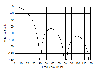 Figure 9-7 Sinc5 Filter Frequency
Response (40 kSPS)
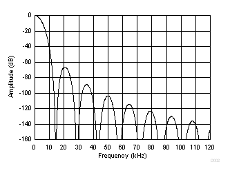 Figure 9-8 Sinc5 Filter Frequency
Response (14.4 kSPS)
Figure 9-8 Sinc5 Filter Frequency
Response (14.4 kSPS)The second stage filter superimposes additional nulls to the nulls produced by the first stage. The first of the nulls occurs at the output data rate with additional nulls occurring at data rate multiples.
Figure 9-9 shows the frequency response at 2.4 kSPS. This data rate has five equally spaced nulls between the first stage 14.4-kHz nulls [(14.4 kHz / 2.4 kHz) – 1 = 5]. This frequency response is similar to that of data rates 2.5 SPS to 7.2 kSPS. Figure 9-10 shows the frequency response nulls at 10 SPS.
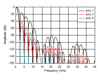 Figure 9-9 Sinc Filter Frequency
Response (2400 SPS)
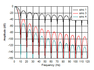 Figure 9-10 Sinc Filter Frequency
Response (10 SPS)
Figure 9-10 Sinc Filter Frequency
Response (10 SPS)Figure 9-11 and Figure 9-12 show the frequency response of data rates 50 SPS and 60 SPS. 50-Hz or 60-Hz rejection is increased by increasing the order of the sinc filter.
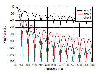 Figure 9-11 Sinc Filter Frequency
Response (50 SPS)
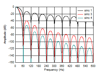 Figure 9-12 Sinc Filter Frequency
Response (60 SPS)
Figure 9-12 Sinc Filter Frequency
Response (60 SPS)Figure 9-13 and Figure 9-14 show the detailed frequency response of the 50-SPS and 60-SPS data rates.
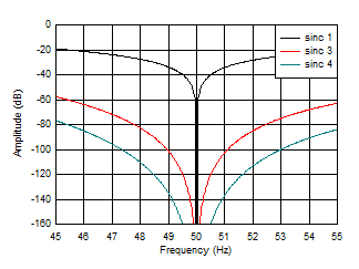 Figure 9-13 Sinc Filter Frequency
Response (50 SPS)
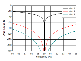 Figure 9-14 Sinc Filter Frequency
Response (60 SPS)
Figure 9-14 Sinc Filter Frequency
Response (60 SPS)The sinc filter has an overall low-pass response that rolls off high-frequency components of the signal. The filter bandwidth depends on the output data rate and the filter order. The system bandwidth is the combined bandwidths of the digital filter, the PGA antialias filter, and external signal filters. Table 9-3 lists the –3-dB bandwidth of the sinc filter.
| –3-dB BANDWIDTH (Hz) | ||||
|---|---|---|---|---|
| DATA RATE (SPS) | SINC1 | SINC3 | SINC4 | SINC5 |
| 2.5 | 1.10 | 0.65 | 0.58 | — |
| 5 | 2.23 | 1.33 | 1.15 | — |
| 10 | 4.43 | 2.62 | 2.28 | — |
| 16.6 | 7.38 | 4.37 | 3.80 | — |
| 20 | 8.85 | 5.25 | 4.63 | — |
| 50 | 22.1 | 13.1 | 11.4 | — |
| 60 | 26.6 | 15.7 | 13.7 | — |
| 100 | 44.3 | 26.2 | 22.8 | — |
| 400 | 177 | 105 | 91.0 | — |
| 1200 | 525 | 314 | 273 | — |
| 2400 | 1015 | 623 | 544 | — |
| 4800 | 1798 | 1214 | 1077 | — |
| 7200 | 2310 | 1750 | 1590 | — |
| 14400 | — | — | — | 2940 |
| 19200 | — | — | — | 3920 |
| 25600 | — | — | — | 5227 |
| 40000 | — | — | — | 8167 |