JAJSGE8B March 2016 – October 2018 ADS1282-SP
PRODUCTION DATA.
- 1 特長
- 2 アプリケーション
- 3 概要
- 4 改訂履歴
- 5 概要(続き)
- 6 Pin Configuration and Functions
-
7 Specifications
- 7.1 Absolute Maximum Ratings
- 7.2 ESD Ratings
- 7.3 Recommended Operating Conditions
- 7.4 Thermal Information
- 7.5 Electrical Characteristics
- 7.6 Timing Requirements
- 7.7 Pulse-Sync Timing Requirements
- 7.8 Reset Timing Requirements
- 7.9 Read Data Timing Requirements
- 7.10 Switching Characteristics
- 7.11 Typical Characteristics
-
8 Detailed Description
- 8.1 Overview
- 8.2 Functional Block Diagram
- 8.3
Feature Description
- 8.3.1 Noise Performance
- 8.3.2 Input-Referred Noise
- 8.3.3 Idle Tones
- 8.3.4 Operating Mode
- 8.3.5 Analog Inputs and Multiplexer
- 8.3.6 PGA (Programmable Gain Amplifier)
- 8.3.7 ADC
- 8.3.8 Modulator
- 8.3.9 Modulator Over-Range
- 8.3.10 Modulator Input Impedance
- 8.3.11 Modulator Over-Range Detection (MFLAG)
- 8.3.12 Voltage Reference Inputs (VREFP, VREFN)
- 8.3.13 Digital Filter
- 8.3.14 Master Clock Input (CLK)
- 8.3.15 Synchronization (SYNC Pin and Sync Command)
- 8.3.16 Pulse-Sync Mode
- 8.3.17 Continuous-Sync Mode
- 8.3.18 Reset (RESET Pin and Reset Command)
- 8.3.19 Power-Down (PWDN Pin and Standby Command)
- 8.3.20 Power-On Sequence
- 8.3.21 Serial Interface
- 8.3.22 Data Format
- 8.3.23 Reading Data
- 8.3.24 One-Shot Operation
- 8.4 Device Functional Modes
- 8.5
Programming
- 8.5.1
Commands
- 8.5.1.1 WAKEUP: Wake-Up from Standby Mode
- 8.5.1.2 STANDBY: Standby Mode
- 8.5.1.3 SYNC: Synchronize the A/D Conversion
- 8.5.1.4 RESET: Reset the Device
- 8.5.1.5 RDATAC: Read Data Continuous
- 8.5.1.6 SDATAC: Stop Read Data Continuous
- 8.5.1.7 RDATA: Read Data By Command
- 8.5.1.8 RREG: Read Register Data
- 8.5.1.9 WREG: Write to Register
- 8.5.1.10 OFSCAL: Offset Calibration
- 8.5.1.11 GANCAL: Gain Calibration
- 8.5.2 Calibration Commands
- 8.5.3 User Calibration
- 8.5.4 Configuration Guide
- 8.5.1
Commands
- 8.6 Register Maps
- 9 Application and Implementation
- 10Power Supply Recommendations
- 11Layout
- 12デバイスおよびドキュメントのサポート
- 13メカニカル、パッケージ、および注文情報
8.3.6 PGA (Programmable Gain Amplifier)
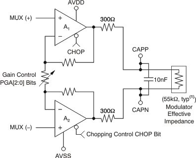
The PGA of the ADS1282-SP is a low-noise, continuous-time, differential-in/differential-out CMOS amplifier. The gain is programmable from 1 to 64, set by register bits, PGA[2:0]. The PGA differentially drives the modulator through 300-Ω internal resistors. A COG capacitor (10 nF typical) must be connected to CAPP and CAPN to filter modulator sampling glitches. The external capacitor also serves as an anti-alias filter. The corner frequency is given in Equation 3:

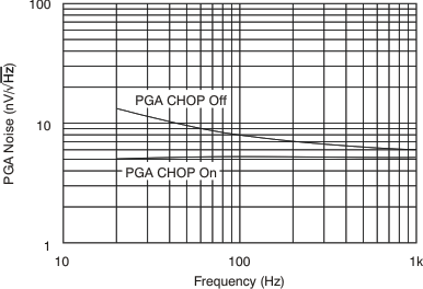
Referring to Figure 29, amplifiers A1 and A2 are chopped to remove the offset, offset drift, and the 1/f noise. Chopping moves the effects to ƒCLK/128 (8 kHz), which is safely out of the passband. Chopping can be disabled by setting the CHOP register bit = 0. With chopping disabled, the impedance of the PGA increases substantially (>> 1 GΩ). As shown in Figure 30, chopping maintains flat noise density; if chopping is disabled, however, it results in a rising 1/f noise profile.
The PGA has programmable gains from 1 to 64. Table 3 shows the register bit setting for the PGA and resulting full-scale differential range.
The specified output operating range of the PGA is shown in Equation 4:
PGA output levels (signal plus common-mode) should be maintained within these limits for best operation.
Table 3. PGA Gain Settings
| PGA[2:0] | GAIN | DIFFERENTIAL INPUT RANGE (V)(1) |
|---|---|---|
| 000 | 1 | ±2.5 |
| 001 | 2 | ±1.25 |
| 010 | 4 | ±0.625 |
| 011 | 8 | ±0.312 |
| 100 | 16 | ±0.156 |
| 101 | 32 | ±0.078 |
| 110 | 64 | ±0.039 |
 Figure 29. PGA Block Diagram
  Figure 30. PGA Noise