JAJSGE8B March 2016 – October 2018 ADS1282-SP
PRODUCTION DATA.
- 1 特長
- 2 アプリケーション
- 3 概要
- 4 改訂履歴
- 5 概要(続き)
- 6 Pin Configuration and Functions
-
7 Specifications
- 7.1 Absolute Maximum Ratings
- 7.2 ESD Ratings
- 7.3 Recommended Operating Conditions
- 7.4 Thermal Information
- 7.5 Electrical Characteristics
- 7.6 Timing Requirements
- 7.7 Pulse-Sync Timing Requirements
- 7.8 Reset Timing Requirements
- 7.9 Read Data Timing Requirements
- 7.10 Switching Characteristics
- 7.11 Typical Characteristics
-
8 Detailed Description
- 8.1 Overview
- 8.2 Functional Block Diagram
- 8.3
Feature Description
- 8.3.1 Noise Performance
- 8.3.2 Input-Referred Noise
- 8.3.3 Idle Tones
- 8.3.4 Operating Mode
- 8.3.5 Analog Inputs and Multiplexer
- 8.3.6 PGA (Programmable Gain Amplifier)
- 8.3.7 ADC
- 8.3.8 Modulator
- 8.3.9 Modulator Over-Range
- 8.3.10 Modulator Input Impedance
- 8.3.11 Modulator Over-Range Detection (MFLAG)
- 8.3.12 Voltage Reference Inputs (VREFP, VREFN)
- 8.3.13 Digital Filter
- 8.3.14 Master Clock Input (CLK)
- 8.3.15 Synchronization (SYNC Pin and Sync Command)
- 8.3.16 Pulse-Sync Mode
- 8.3.17 Continuous-Sync Mode
- 8.3.18 Reset (RESET Pin and Reset Command)
- 8.3.19 Power-Down (PWDN Pin and Standby Command)
- 8.3.20 Power-On Sequence
- 8.3.21 Serial Interface
- 8.3.22 Data Format
- 8.3.23 Reading Data
- 8.3.24 One-Shot Operation
- 8.4 Device Functional Modes
- 8.5
Programming
- 8.5.1
Commands
- 8.5.1.1 WAKEUP: Wake-Up from Standby Mode
- 8.5.1.2 STANDBY: Standby Mode
- 8.5.1.3 SYNC: Synchronize the A/D Conversion
- 8.5.1.4 RESET: Reset the Device
- 8.5.1.5 RDATAC: Read Data Continuous
- 8.5.1.6 SDATAC: Stop Read Data Continuous
- 8.5.1.7 RDATA: Read Data By Command
- 8.5.1.8 RREG: Read Register Data
- 8.5.1.9 WREG: Write to Register
- 8.5.1.10 OFSCAL: Offset Calibration
- 8.5.1.11 GANCAL: Gain Calibration
- 8.5.2 Calibration Commands
- 8.5.3 User Calibration
- 8.5.4 Configuration Guide
- 8.5.1
Commands
- 8.6 Register Maps
- 9 Application and Implementation
- 10Power Supply Recommendations
- 11Layout
- 12デバイスおよびドキュメントのサポート
- 13メカニカル、パッケージ、および注文情報
8.3.13.2 FIR Stage
The second stage of the ADS1282-SP digital filter is an FIR low-pass filter. Data are supplied to this stage from the sinc filter. The FIR stage is segmented into four sub-stages, as shown in Figure 39. The first two sub-stages are half-band filters with decimation ratios of 2. The third sub-stage decimates by 4 and the fourth sub-stage decimates by 2. The overall decimation of the FIR stage is 32. Two coefficient sets are used for the third and fourth sections, depending on the phase selection. Table 20 (in デバイス・サポート) lists the FIR stage coefficients. Table 6 lists the data rates and overall decimation ratio of the FIR stage.
Table 6. Fir Filter Data Rates
| DR[2:0] REGISTER | DECIMATION RATIO (N) | FIR DATA RATE (SPS) |
|---|---|---|
| 000 | 4096 | 250 |
| 001 | 2048 | 500 |
| 010 | 1024 | 1000 |
| 011 | 512 | 2000 |
| 100 | 256 | 4000 |
 Figure 39. Fir Filter Sub-Stages
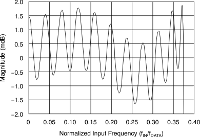
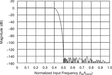
 As shown in Figure 40, the FIR frequency response provides a flat passband to 0.375 of the data rate (±0.003-dB passband ripple). Figure 41 shows the transition from passband to stop band.
 Figure 40. FIR Passband Magnitude Response (FDATA = 500 Hz)
  Figure 41. FIR Transition Band Magnitude Response
 Although not shown in Figure 41, the passband response repeats at multiples of the modulator frequency (NƒMOD – ƒ0 and NƒMOD + ƒ0, where N = 1, 2, and so forth, and ƒ0 = passband). These image frequencies, if present in the signal and not externally filtered, fold back (or alias) into the passband and cause errors. A low-pass signal filter reduces the effect of aliasing. Often, the RC low-pass filter provided by the PGA output resistors and the external capacitor connected to CAPP and CAPN provides sufficient signal attenuation.