JAJSHV5B June 2017 – August 2019 ADS1287
PRODUCTION DATA.
- 1 特長
- 2 アプリケーション
- 3 概要
- 4 改訂履歴
- 5 概要(続き)
- 6 Pin Configuration and Functions
- 7 Specifications
- 8 Parameter Measurement Information
-
9 Detailed Description
- 9.1 Overview
- 9.2 Functional Block Diagram
- 9.3 Feature Description
- 9.4 Device Functional Modes
- 9.5
Programming
- 9.5.1 Serial Interface
- 9.5.2
Commands
- 9.5.2.1 WAKEUP: Wake Up Command
- 9.5.2.2 STANDBY: Standby Mode Command
- 9.5.2.3 SYNC: Synchronize ADC Conversions
- 9.5.2.4 RESET: Reset Command
- 9.5.2.5 RDATAC: Read Data Continuous Mode Command
- 9.5.2.6 SDATAC: Stop Read Data Continuous Mode Command
- 9.5.2.7 RDATA: Read Data Command
- 9.5.2.8 RREG: Read Register Data Command
- 9.5.2.9 WREG: Write Register Data Command
- 9.5.2.10 OFSCAL: Offset Calibration Command
- 9.5.2.11 GANCAL: Gain Calibration Command
- 9.6
Register Map
- 9.6.1
Register Descriptions
- 9.6.1.1 ID/CFG: ID, Configuration Register (address = 00h) [reset = x0h]
- 9.6.1.2 CONFIG0: Configuration Register 0 (address = 01h) [reset = 52h]
- 9.6.1.3 CONFIG1: Configuration Register 1 (address = 02h) [reset = 08h]
- 9.6.1.4 High-Pass Filter Corner Frequency (HPFx) Registers (address = 03h, 04h) [reset = 32h, 03h]
- 9.6.1.5 Offset Calibration (OFCx) Registers (address = 05h, 06h, 07h) [reset = 00h, 00h, 00h]
- 9.6.1.6 Full-Scale Calibration (FSCx) Registers (address = 08h, 09h, 0Ah) [reset = 00h, 00h, 40h]
- 9.6.1
Register Descriptions
- 10Application and Implementation
- 11Power Supply Recommendations
- 12Layout
- 13デバイスおよびドキュメントのサポート
- 14メカニカル、パッケージ、および注文情報
パッケージ・オプション
デバイスごとのパッケージ図は、PDF版データシートをご参照ください。
メカニカル・データ(パッケージ|ピン)
- RHF|24
サーマルパッド・メカニカル・データ
発注情報
7.7 Switching Characteristics
over operating ambient temperature range, DVDD = 2.25 V to 3.6 V, and DOUT loading = 20 pF || 100 kΩ (unless otherwise noted)| PARAMETER | TEST CONDITIONS | MIN | TYP | MAX | UNIT | |
|---|---|---|---|---|---|---|
| SERIAL INTERFACE | ||||||
| tp(DRDO) | Propagation delay time,
DRDY falling edge to valid data DOUT |
100 | ns | |||
| tp(CSDOD) | Propagation delay time,
CS falling edge to DOUT driven |
60 | ns | |||
| tp(SCDO1) | Propagation delay time,
SCLK falling edge to valid new DOUT |
100 | ns | |||
| tp(SCDO2) | Propagation delay time,
SCLK falling edge to valid old DOUT |
0 | ns | |||
| tp(CSDOZ) | Propagation delay time,
CS rising edge to DOUT Hi-z |
40 | ns | |||
| tw(DRH) | Pulse duration, DRDY high | 4 | 1 / fCLK | |||
| tp(CMDR) | Propagation delay time, RDATA command to DRDY low (see Figure 60) | 0 | 1 | 1 / fDATA | ||
| SYNCHRONIZATION | ||||||
| tp(SYDR) | Propagation delay time, SYNC rising edge to DRDY falling edge | High-resolution mode, 62.5 SPS | 1008.145 | ms(1) | ||
| High-resolution mode, 125 SPS | 504.301 | |||||
| High-resolution mode, 250 SPS | 252.379 | |||||
| High-resolution mode, 500 SPS | 126.419 | |||||
| High-resolution mode, 1000 SPS | 63.438 | |||||
| Low-power mode, 62.5 SPS | 1008.390 | |||||
| Low-power mode, 125 SPS | 504.548 | |||||
| Low-power mode, 250 SPS | 252.625 | |||||
| Low-power mode, 500 SPS | 126.665 | |||||
| Low-power mode, 1000 SPS | 63.684 | |||||
| Sinc filter and high-resolution mode, 2000 SPS | 2.755 | |||||
| Sinc filter and high-resolution mode, 4000 SPS | 1.630 | |||||
| Sinc filter and high-resolution mode, 8000 SPS | 0.942 | |||||
| Sinc filter and high-resolution mode, 16000 SPS | 0.599 | |||||
| Sinc filter and high-resolution mode, 32000 SPS | 0.427 | |||||
| RESET | ||||||
| tp(RSDR) | Propagation delay time, RESET pin or reset command to DRDY falling edge | 252.379 | ms | |||
| POWER-DOWN MODE and STANDBY MODE WAKEUP | ||||||
| tp(PWDR) | Propagation delay time, exit power-down or standby mode to first data ready | 252.379(2) | ms | |||
| POWER-UP | ||||||
| tp(PUCM) | Propagation delay time, power-on threshold voltage to communication ready | 216 | fCLK | |||
| tp(PUDR) | Propagation delay time, power-on threshold voltage to first data ready | 216 / fCLK + 252.379 | ms(1) | |||
(1) fCLK = 1.024 MHz.
(2) The exit power-down mode default setting is 250 SPS with the FIR filter mode. Subtract two fCLK cycles for a WAKEUP command. The WAKEUP command is timed from the rising CLK edge after the eighth rising SCLK edge.
 Figure 1. Serial Interface Timing Requirements
 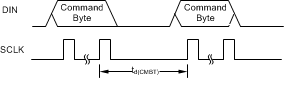 Figure 2. Serial Interface Command Timing Requirements
  Figure 3. Serial Interface Switching Characteristics
 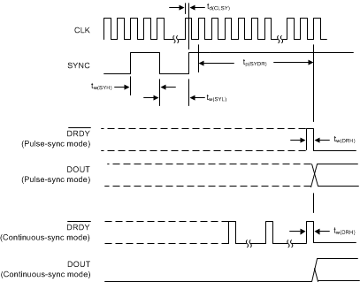 Figure 4. Synchronization Timing
 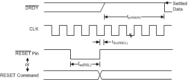 Figure 5. Reset Timing
 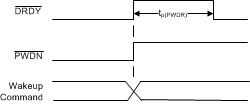 Figure 6. Power-Down and Standby Wake-Up Timing
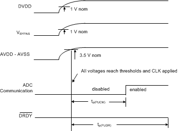 Figure 7. Power-Up Timing