JAJSPW8E march   2011  – february 2023 ADS4222 , ADS4225 , ADS4226 , ADS4242 , ADS4245 , ADS4246

PRODUCTION DATA  

  1. 特長
  2. アプリケーション
  3. 概要
  4. Revision History
  5. 概要 (続き)
  6. Pin Configuration and Functions
    1.     Pin Functions – LVDS Mode
    2.     Pin Functions – CMOS Mode
  7. Specifications
    1. 7.1  Absolute Maximum Ratings
    2. 7.2  ESD Ratings
    3. 7.3  Recommended Operating Conditions
    4. 7.4  Thermal Information
    5. 7.5  Electrical Characteristics: ADS4246, ADS4245, ADS4242
    6. 7.6  Electrical Characteristics: ADS4226, ADS4225, ADS4222
    7. 7.7  Electrical Characteristics: General
    8. 7.8  Digital Characteristics
    9. 7.9  Timing Requirements: LVDS and CMOS Modes #GUID-C6C0701B-A11B-492F-BD6B-B774F5FE4665/SLAS6895399
    10. 7.10 Serial Interface Timing Characteristics #GUID-3852E7CE-C5B6-42F5-A56A-70AB1B981302/SBAS5097810
    11. 7.11 Reset Timing (Only When Serial Interface Is Used)
    12. 7.12 Typical Characteristics
      1. 7.12.1 ADS4246
      2. 7.12.2 ADS4245
      3. 7.12.3 ADS4242
      4. 7.12.4 ADS4226
      5. 7.12.5 ADS4225
      6. 7.12.6 ADS4222
      7. 7.12.7 General
      8. 7.12.8 Contour
  8. Detailed Description
    1. 8.1 Overview
    2. 8.2 Functional Block Diagrams
    3. 8.3 Feature Description
      1. 8.3.1 Analog Input
        1. 8.3.1.1 Drive Circuit Requirements
        2. 8.3.1.2 Driving Circuit
      2. 8.3.2 Clock Input
      3. 8.3.3 Digital Functions
      4. 8.3.4 Gain for SFDR/SNR Trade-off
      5. 8.3.5 Offset Correction
    4. 8.4 Device Functional Modes
      1. 8.4.1 Power-Down
        1. 8.4.1.1 Global Power-Down
        2. 8.4.1.2 Channel Standby
        3. 8.4.1.3 Input Clock Stop
    5. 8.5 Programming
      1. 8.5.1 47
      2. 8.5.2 Parallel Configuration Only
      3. 8.5.3 Serial Interface Configuration Only
      4. 8.5.4 Using Both Serial Interface and Parallel Controls
      5. 8.5.5 Parallel Configuration Details
      6. 8.5.6 Serial Interface Details
        1. 8.5.6.1 Register Initialization
        2. 8.5.6.2 Serial Register Readout
      7. 8.5.7 Digital Output Information
        1. 8.5.7.1 Output Interface
        2. 8.5.7.2 DDR LVDS Outputs
        3. 8.5.7.3 LVDS Buffer
        4. 8.5.7.4 Parallel CMOS Interface
        5. 8.5.7.5 CMOS Interface Power Dissipation
        6. 8.5.7.6 Multiplexed Mode of Operation
        7. 8.5.7.7 Output Data Format
    6. 8.6 Register Maps
      1. 8.6.1 64
      2. 8.6.2 Description Of Serial Registers
  9. Application and Implementation
    1. 9.1 Application Information
    2. 9.2 Typical Application
      1. 9.2.1 Design Requirements
      2. 9.2.2 Detailed Design Procedure
        1. 9.2.2.1 Analog Input
        2. 9.2.2.2 Clock Driver
        3. 9.2.2.3 Digital Interface
        4. 9.2.2.4 SNR and Clock Jitter
      3. 9.2.3 Application Curves
    3. 9.3 Power Supply Recommendations
      1. 9.3.1 Sharing DRVDD and AVDD Supplies
      2. 9.3.2 Using DC/DC Power Supplies
      3. 9.3.3 Power Supply Bypassing
    4. 9.4 Layout
      1. 9.4.1 Layout Guidelines
        1. 9.4.1.1 Grounding
        2. 9.4.1.2 Supply Decoupling
        3. 9.4.1.3 Exposed Pad
        4. 9.4.1.4 Routing Analog Inputs
      2. 9.4.2 Layout Example
  10. 10Device and Documentation Support
    1. 10.1 Device Support
      1. 10.1.1 Device Nomenclature
    2. 10.2 Documentation Support
      1. 10.2.1 Related Documentation
    3. 10.3 サポート・リソース
    4. 10.4 商標
    5. 10.5 静電気放電に関する注意事項
    6. 10.6 用語集
  11. 11Mechanical, Packaging, and Orderable Information

パッケージ・オプション

メカニカル・データ(パッケージ|ピン)
サーマルパッド・メカニカル・データ
発注情報

SNR and Clock Jitter

The signal-to-noise ratio (SNR) of the ADC is limited by three different factors, as shown in Equation 1. Quantinization noise is typically not noticeable in pipeline converters and is 96 dBFS for a 16-bit ADC. Thermal noise limits SNR at low input frequencies and clock jitter sets SNR for higher input frequencies.

Equation 1. GUID-4F678B67-942C-4611-9190-123C61E9938F-low.gif

SNR limitation is a result of sample clock jitter and can be calculated by Equation 2

Equation 2. GUID-D34C4A28-7ACA-4A3A-81FE-0CE1BC7542B2-low.gif

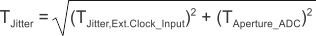
The total clock jitter (TJitter) has three components: the internal aperture jitter (85 fs for the device) is set by the noise of the clock input buffer, the external clock jitter, and the jitter from the analog input signal. TJitter can be calculated by Equation 3:

Equation 3. GUID-BF16BA62-F038-423D-A937-3E5D5BFC8099-low.gif

External clock jitter can be minimized by using high-quality clock sources and jitter cleaners as well as band-pass filters at the clock input while a faster clock slew rate improved ADC aperture jitter. The device has a 74.1-dBFS thermal noise and an 85-fS internal aperture jitter. The SNR value depends on the amount of external jitter for different input frequencies, as shown in Figure.

GUID-2F193C32-BFCE-4E56-A212-4922AF3F5E85-low.gifFigure 9-2 SNR versus Input Frequency and External Clock Jitter