JAJSJG5 July   2020 ADS9226

PRODUCTION DATA  

  1. 特長
  2. アプリケーション
  3. 概要
  4. Revision History
  5. Pin Configuration and Functions
    1.     Pin Functions
  6. Specifications
    1. 6.1 Absolute Maximum Ratings
    2. 6.2 ESD Ratings
    3. 6.3 Recommended Operating Conditions
    4. 6.4 Thermal Information
    5. 6.5 Electrical Characteristics
    6. 6.6 Timing Requirements
    7. 6.7 Switching Characteristics
    8. 6.8 Timing Diagrams
    9. 6.9 Typical Characteristics
  7. Detailed Description
    1. 7.1 Overview
    2. 7.2 Functional Block Diagram
    3. 7.3 Feature Description
      1. 7.3.1 Converter Modules
        1. 7.3.1.1 Analog Input With Sample-and-Hold
        2. 7.3.1.2 ADC Transfer Function
      2. 7.3.2 External Reference Voltage
      3. 7.3.3 Reference Buffers
    4. 7.4 Device Functional Modes
      1. 7.4.1 ACQ State
      2. 7.4.2 CNV State
      3. 7.4.3 Output Data Word
      4. 7.4.4 Conversion Control and Data Transfer Frame
  8. Application and Implementation
    1. 8.1 Application Information
      1. 8.1.1 ADC Input Driver
        1. 8.1.1.1 Charge-Kickback Filter
      2. 8.1.2 Input Amplifier Selection
    2. 8.2 Typical Application
      1. 8.2.1 Design Requirements
      2. 8.2.2 Detailed Design Procedure
      3. 8.2.3 Application Curve
  9. Power Supply Recommendations
  10. 10Layout
    1. 10.1 Layout Guidelines
      1. 10.1.1 Signal Path
      2. 10.1.2 Grounding and PCB Stack-Up
      3. 10.1.3 Decoupling of Power Supplies
      4. 10.1.4 Reference Decoupling
      5. 10.1.5 Analog Input Decoupling
    2. 10.2 Layout Example
  11. 11Device and Documentation Support
    1. 11.1 Related Documentation
    2. 11.2 Receiving Notification of Documentation Updates
    3. 11.3 サポート・リソース
    4. 11.4 Trademarks
    5. 11.5 静電気放電に関する注意事項
    6. 11.6 用語集
  12. 12Mechanical, Packaging, and Orderable Information

パッケージ・オプション

メカニカル・データ(パッケージ|ピン)
サーマルパッド・メカニカル・データ
発注情報

Conversion Control and Data Transfer Frame

A data transfer frame starts with a falling edge of the CS signal. In any frame, the clocks provided on the SCLK pin are used to transfer the output data for the completed conversion. The device has two SDOs (SDO-0x and SDO-1x) for each ADC. For ADC_A, the device provides data on SDO-0A and SDO-1A, whereas for ADC_B, the device provides data on SDO-0B and SDO-1B. The most significant bit (Dn-1x) of the output data is launched on the SDO-1x pins and the MSB-1 (Dn-2x) bit is launched on the SDO-0x pins on the falling edge of CS, any subsequent output bits are launched on the rising edges provided on SCLK. When all output bits of the conversion result are shifted out, the device launches 0's on the subsequent SCLK rising edges. The data transfer frame ends with a rising edge of the CS signal. For detailed timing specifications, see Section 6 and Figure 7-6.

The CS pulse high time determines if the data being read back is with a 0 sample latency or a 1 sample latency. See Figure 6-1 and Figure 6-2 for the respective timing diagrams. The maximum-rated sampling rate of 2.048 MSPS is achieved with a latency-1 data capture.
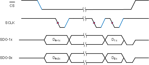
GUID-EE24EA61-24E8-4C0D-A06C-8A3115F19189-low.gif
For ADC_A, x = A. For ADC_B, x = B.
Figure 7-6 Data Transfer Frame for Reading Data