JAJSNC3 March   2024 AFE7950-SP

PRODMIX  

  1.   1
  2. 1特長
  3. 2アプリケーション
  4. 3概要
  5. 4Specifications
    1. 4.1  Absolute Maximum Ratings
    2. 4.2  ESD Ratings
    3. 4.3  Recommended Operating Conditions
    4. 4.4  Thermal Information
    5. 4.5  Transmitter Electrical Characteristics
    6. 4.6  RF ADC Electrical Characteristics
    7. 4.7  PLL/VCO/Clock Electrical Characteristics
    8. 4.8  Digital Electrical Characteristics
    9. 4.9  Power Supply Electrical Characteristics
    10. 4.10 Timing Requirements
    11. 4.11 Switching Characteristics
    12. 4.12 Typical Characteristics
      1. 4.12.1  TX Typical Characteristics 800MHz
      2. 4.12.2  TX Typical Characteristics at 1.8GHz
      3. 4.12.3  TX Typical Characteristics at 2.6GHz
      4. 4.12.4  TX Typical Characteristics at 3.5GHz
      5. 4.12.5  TX Typical Characteristics at 4.9GHz
      6. 4.12.6  TX Typical Characteristics at 8.1GHz
      7. 4.12.7  TX Typical Characteristics at 9.6GHz
      8. 4.12.8  RX Typical Characteristics at 800MHz
      9. 4.12.9  RX Typical Characteristics at 1.75-1.9GHz
      10. 4.12.10 RX Typical Characteristics at 2.6GHz
      11. 4.12.11 RX Typical Characteristics at 3.5GHz
      12. 4.12.12 RX Typical Characteristics at 4.9GHz
      13. 4.12.13 RX Typical Characteristics at 8.1GHz
      14. 4.12.14 RX Typical Characteristics at 9.6GHz
  6. 5Device and Documentation Support
    1. 5.1 ドキュメントの更新通知を受け取る方法
    2. 5.2 サポート・リソース
    3. 5.3 Trademarks
    4. 5.4 静電気放電に関する注意事項
    5. 5.5 用語集
  7. 6Revision History
  8. 7Mechanical, Packaging, and Orderable Information

パッケージ・オプション

メカニカル・データ(パッケージ|ピン)
サーマルパッド・メカニカル・データ
発注情報

TX Typical Characteristics at 1.8GHz

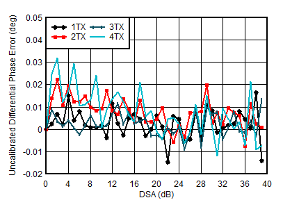
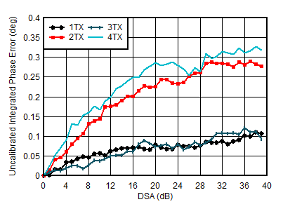
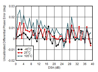
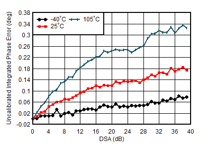
Typical values at TA = +25°C with nominal supplies. Default conditions: TX input data rate = 491.52MSPS, fDAC = 11796.48MSPS (24x interpolation), interleave mode, 1st Nyquist zone output, PLL clock mode with fREF = 491.52MHz, AOUT = –1 dBFS, DSA = 0dB, Sin(x)/x enabled, DSA calibrated
GUID-8C29C0AB-91CD-44B1-919A-4FAAFE568301-low.gif
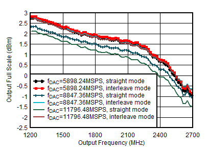
including PCB and cable losses, Aout = -0.5dFBS, DSA = 0, 1.8GHz matching
Figure 4-44 TX Output Fullscale vs Output Frequency
GUID-31400215-312E-42B5-86F3-12DBAC10E7A2-low.gif
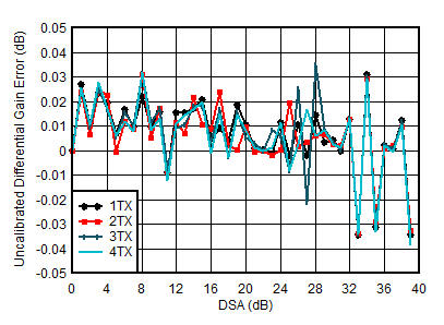
fDAC = 5898.24MSPS, interleave mode, matching at 1.8GHz
Differential Gain Error = POUT(DSA Setting – 1) – POUT(DSA Setting) + 1
Figure 4-46 TX Uncalibrated Differential Gain Error vs DSA Setting and Channel at 1.8GHz
GUID-32A36896-22F2-4588-BFB4-9A3826EFCF5F-low.gif
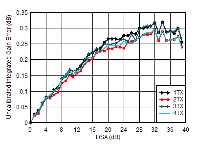
fDAC = 5898.24MSPS, interleave mode, matching at 1.8GHz
Integrated Gain Error = POUT(DSA Setting) – POUT(DSA Setting = 0) + (DSA Setting)
Figure 4-48 TX Uncalibrated Integrated Gain Error vs DSA Setting and Channel at 1.8GHz
GUID-4D62AE58-26B6-44C3-82D9-C5A812551A79-low.gif
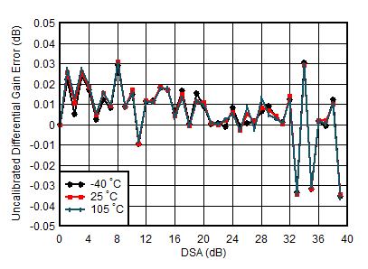
fDAC = 5898.24MSPS, interleave mode, matching at 1.8GHz
Differential Gain Error = POUT(DSA Setting – 1) – POUT(DSA Setting) + 1
Figure 4-50 TX Uncalibrated Differential Gain Error vs DSA Setting and Temperature at 1.8GHz
GUID-76AA1407-8E4B-4C6A-81CB-CB75BC66596D-low.gif
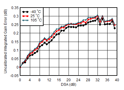
fDAC = 5898.24MSPS, interleave mode, matching at 1.8GHz
Integrated Gain Error = POUT(DSA Setting) – POUT(DSA Setting = 0) + (DSA Setting)
Figure 4-52 TX Uncalibrated Integrated Gain Error vs DSA Setting and Temperature at 1.8GHz
GUID-C243D5C7-1C9F-4EFC-BE11-3AADBB370844-low.gif
fDAC = 5898.24MSPS, interleave mode, matching at 1.8GHz
Differential Phase Error = PhaseOUT(DSA Setting – 1) – PhaseOUT(DSA Setting)
Figure 4-54 TX Uncalibrated Differential Phase Error vs DSA Setting and Channel at 1.8GHz
GUID-80CD381E-897F-4629-902C-530FD773DAA0-low.gif
fDAC = 5898.24MSPS, interleave mode, matching at 1.8GHz
Integrated Phase Error = Phase(DSA Setting) – Phase(DSA Setting = 0)
Figure 4-56 TX Uncalibrated Integrated Phase Error vs DSA Setting and Channel at 1.8GHz
GUID-EE8467E6-2061-4F53-A27B-FE98862D0E68-low.gif
fDAC = 5898.24MSPS, interleave mode, matching at 1.8GHz
Differential Phase Error = PhaseOUT(DSA Setting – 1) – PhaseOUT(DSA Setting)
Figure 4-58 TX Uncalibrated Differential Phase Error vs DSA Setting and Temperature at 1.8GHz
GUID-2BA5B0C7-6C3C-4661-BD44-A16455ECE879-low.gif
fDAC = 5898.24MSPS, interleave mode, matching at 1.8GHz, channel with the median variation over DSA setting at 25°C
Integrated Phase Error = Phase(DSA Setting) – Phase(DSA Setting = 0)
Figure 4-60 TX Uncalibrated Integrated Phase Error vs DSA Setting and Temperature at 1.8GHz
GUID-101AF4C6-437B-4667-B2F0-430880F7D239-low.gif
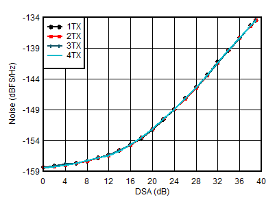
fDAC = 5898.24MSPS, interleave mode, matching at 1.8GHz, POUT = –13dBFS
Figure 4-62 TX Output Noise vs Channel and Attenuation at 1.8GHz
GUID-75F70737-6CB2-49E9-92FA-54ECAFE13401-low.gif
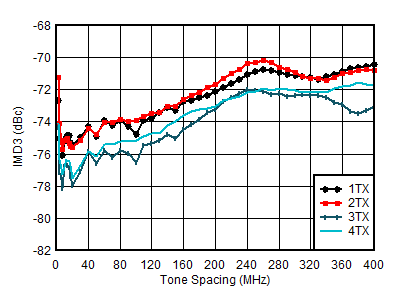
fDAC = 11796.48MSPS, interleave mode, fCENTER = 1.8GHz, matching at 1.8GHz, –13dBFS each tone
Figure 4-64 TX IMD3 vs Tone Spacing and Channel at 1.8GHz
GUID-6859C313-BD69-4FD7-9786-9EF1F311EA0C-low.gif
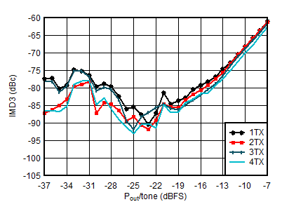
fDAC = 11796.48MSPS, interleave mode, fCENTER = 1.8GHz, fSPACING = 20MHz, matching at 1.8GHz
Figure 4-66 TX IMD3 vs Digital Level at 1.8GHz
GUID-FE913DD7-0F02-4C81-8AAC-D03B329DB8F9-low.gif
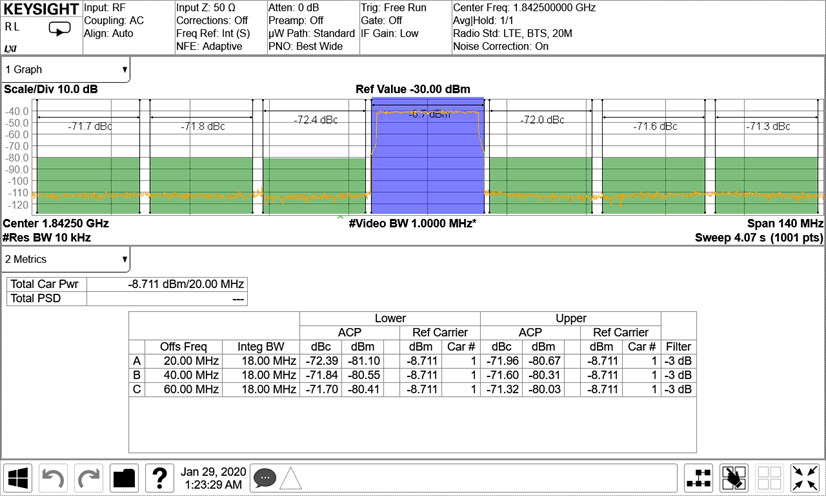
TM1.1, POUT_RMS = –13dBFS
Figure 4-68 TX 20-MHz LTE Output Spectrum at 1.8425GHz
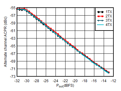
GUID-746DE7E8-3C80-4B29-98AF-C85F7723B297-low.gif
Matching at 1.8GHz, single carrier 20MHz BW TM1.1 LTE
Figure 4-70 TX 20MHz LTE alt-ACPR vs Digital Level at 1.8425GHz
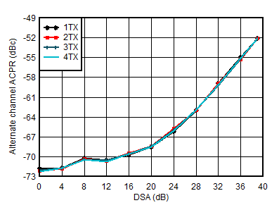
GUID-AFC77E71-9C54-4504-86CB-02E7CDF68FFB-low.gif
Matching at 1.8GHz, single carrier 20MHz BW TM1.1 LTE
Figure 4-72 TX 20MHz LTE alt-ACPR vs DSA at 1.8GHz
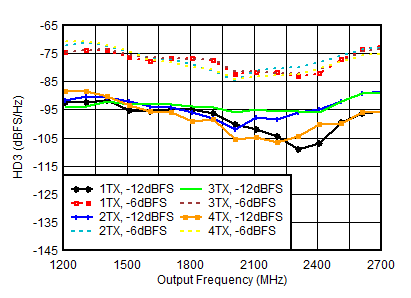
GUID-EB8F4BCD-2D22-4F44-90EE-C4751EBDE752-low.gif
Matching at 1.8GHz, fDAC = 11.79648GSPS, interleave mode, normalized to output power at harmonic frequency
Figure 4-74 TX HD3 vs Digital Amplitude and Output Frequency at 1.8GHz
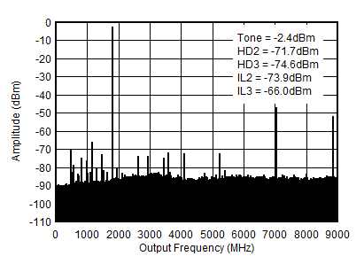
GUID-A4A4B013-1134-4106-9AC7-5E1B8CDABEEC-low.gif
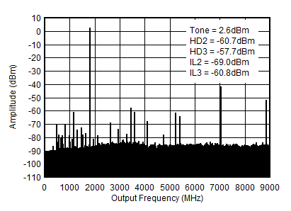
fDAC = 8847.36MSPS, straight mode, 1.8GHz matching, includes PCB and cable losses. ILn = fS/n ± fOUT and is due to mixing with digital clocks.
Figure 4-76 TX Single Tone (–6 dBFS) Output Spectrum at 1.8GHz (0-fDAC)
GUID-980CB847-ECD0-4287-9797-588ADD61D1C6-low.gif
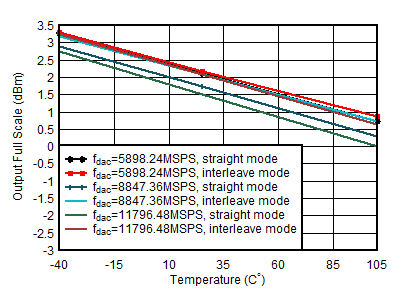
Aout = -0.5dFBS, matching 1.8GHz
Figure 4-45 TX Output Power vs Temperature at 1.8GHz
GUID-2916429E-028A-4AAF-9F68-63E331BA0A45-low.gif
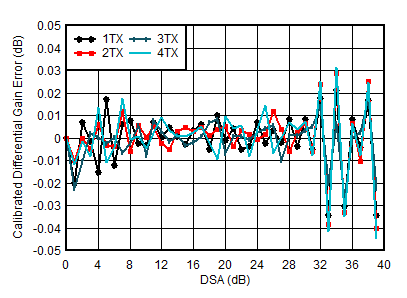
fDAC = 5898.24MSPS, interleave mode, matching at 1.8GHz
Differential Gain Error = POUT(DSA Setting – 1) – POUT(DSA Setting) + 1
Figure 4-47 TX Calibrated Differential Gain Error vs DSA Setting and Channel at 1.8GHz
GUID-13FFB36E-16D6-421E-8348-040806506A28-low.gif
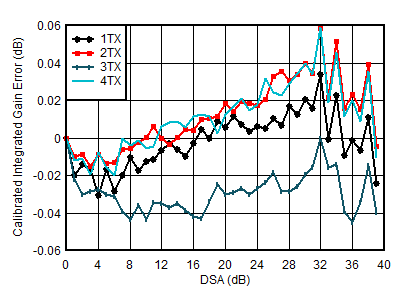
fDAC = 5898.24MSPS, interleave mode, matching at 1.8GHz
Integrated Gain Error = POUT(DSA Setting) – POUT(DSA Setting = 0) + (DSA Setting)
Figure 4-49 TX Calibrated Integrated Gain Error vs DSA Setting and Channel at 1.8GHz
GUID-A6DFD3C0-4C81-494D-8C6F-EA7D0CECE1E2-low.gif
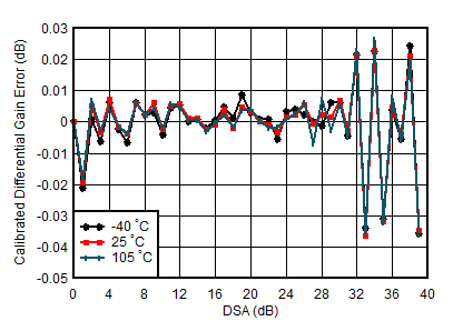
fDAC = 5898.24MSPS, interleave mode, matching at 1.8GHz
Differential Gain Error = POUT(DSA Setting – 1) – POUT(DSA Setting) + 1
Figure 4-51 TX Calibrated Differential Gain Error vs DSA Setting and Temperature at 1.8GHz
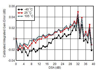
GUID-7F071E5E-C357-46DA-A2CA-720DCE9AB557-low.gif
fDAC = 5898.24MSPS, interleave mode, matching at 1.8GHz
Integrated Gain Error = POUT(DSA Setting) – POUT(DSA Setting = 0) + (DSA Setting)
Figure 4-53 TX Calibrated Integrated Gain Error vs DSA Setting and Temperature at 1.8GHz
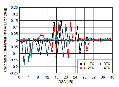
GUID-F973ED55-9DEB-4B05-99B2-9C956F356018-low.gif
fDAC = 8847.36MSPS, straight mode, matching at 2.6GHz
Differential Phase Error = PhaseOUT(DSA Setting – 1) – PhaseOUT(DSA Setting)
Phase DNL spike may occur at any DSA setting.
Figure 4-55 TX Calibrated Differential Phase Error vs DSA Setting and Channel at 1.8GHz
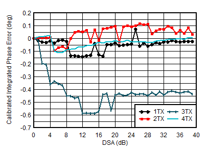
GUID-775B32AE-AB2D-45A1-8D7E-7ED321F95134-low.gif
fDAC = 5898.24MSPS, interleave mode, matching at 1.8GHz
Integrated Phase Error = Phase(DSA Setting) – Phase(DSA Setting = 0)
Figure 4-57 TX Calibrated Integrated Phase Error vs DSA Setting and Channel at 1.8GHz
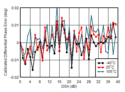
GUID-6113A9A4-4612-4029-A4E6-5ABFC6F09515-low.gif
fDAC = 5898.24MSPS, interleave mode, matching at 1.8GHz, channel with the median variation over DSA setting at 25°C
Differential Phase Error = PhaseOUT(DSA Setting – 1) – PhaseOUT(DSA Setting)
Figure 4-59 TX Calibrated Differential Phase Error vs DSA Setting and Temperature at 1.8GHz
GUID-73EE48FE-8100-46E1-87AA-060C71D1C804-low.gif
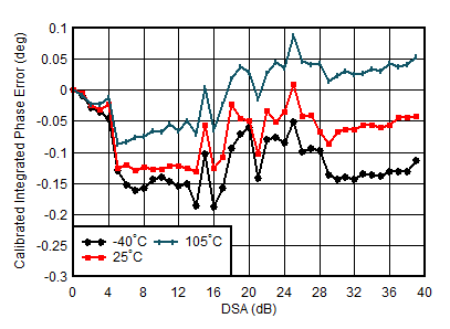
fDAC = 5898.24MSPS, interleave mode, matching at 1.8GHz, channel with the median variation over DSA setting at 25°C
Integrated Phase Error = Phase(DSA Setting) – Phase(DSA Setting = 0)
Figure 4-61 TX Calibrated Integrated Phase Error vs DSA Setting and Temperature at 1.8GHz
GUID-C4C45129-EE86-4A4F-8E8E-4BD675CE5A01-low.gif
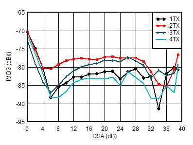
fDAC = 11796.48 MSPS, interleave mode, fCENTER = 1.8GHz, matching at 1.8GHz, –13dBFS each tone
Figure 4-63 TX IMD3 vs DSA Setting at 1.8GHz
GUID-F42EDD78-A334-4858-B166-0D3FE9D61B84-low.gif
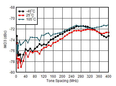
fDAC = 11796.48MSPS, interleave mode, fCENTER = 1. GHz, matching at 1.8GHz, –13dBFS each tone, worst channel
Figure 4-65 TX IMD3 vs Tone Spacing and Temperature at 1.8GHz
GUID-C4C59BF2-01C9-4944-9F8A-CA5016168261-low.gif
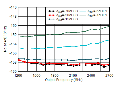
Matching at 2.6GHz, Single tone, fDAC = 11.79648GSPS, interleave mode, 40MHz offset
Figure 4-67 TX Single Tone Output Noise vs Frequency and Amplitude at 1.8GHz
GUID-F71919D1-F695-4DEE-9003-23E87F3F47EF-low.gif
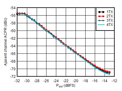
Matching at 1.8GHz, single carrier 20MHz BW TM1.1 LTE
Figure 4-69 TX 20MHz LTE ACPR vs Digital Level at 1.8425GHz
GUID-673BFA61-85A0-4D92-A963-B6B5149242AF-low.gif
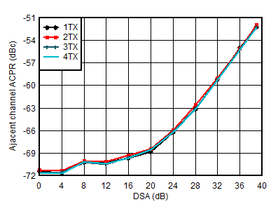
Matching at 1.8GHz, single carrier 20MHz BW TM1.1 LTE
Figure 4-71 TX 20MHz LTE ACPR vs DSA at 1.8GHz
GUID-B1150E72-3C49-4803-9F6E-0124800FDD5A-low.gif
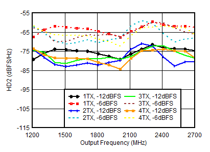
Matching at 1.8GHz, fDAC = 11.79648GSPS, interleave mode, normalized to output power at harmonic frequency
Figure 4-73 TX HD2 vs Digital Amplitude and Output Frequency at 1.8GHz
GUID-5F7B77DD-CF6A-49F4-83EB-F117E4FA43E0-low.gif
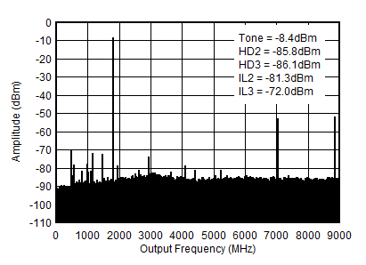
fDAC = 8847.36MSPS, straight mode, 1.8GHz matching, includes PCB and cable losses. ILn = fS/n ± fOUT and is due to mixing with digital clocks.
Figure 4-75 TX Single Tone (–12 dBFS) Output Spectrum at 1.8GHz (0-fDAC)
GUID-6B5BC7B2-C6C2-4635-92A2-77A24B281B9B-low.gif
fDAC = 8847.36MSPS, straight mode, 1.8GHz matching, includes PCB and cable losses. ILn = fS/n ± fOUT and is due to mixing with digital clocks.
Figure 4-77 TX Single Tone (–1dBFS) Output Spectrum at 1.8GHz (0-fDAC)