JAJSN92 December   2022 AFE78101 , AFE88101

PRODUCTION DATA  

  1. 特長
  2. アプリケーション
  3. 概要
  4. Revision History
  5. Pin Configuration and Functions
  6. Specifications
    1. 6.1  Absolute Maximum Ratings
    2. 6.2  ESD Ratings
    3. 6.3  Recommended Operating Conditions
    4. 6.4  Thermal Information
    5. 6.5  Electrical Characteristics
    6. 6.6  Timing Requirements
    7. 6.7  Timing Diagrams
    8. 6.8  Typical Characteristics: VOUT DAC
    9. 6.9  Typical Characteristics: ADC
    10. 6.10 Typical Characteristics: Reference
    11. 6.11 Typical Characteristics: Power Supply
  7. Detailed Description
    1. 7.1 Overview
    2. 7.2 Functional Block Diagram
    3. 7.3 Feature Description
      1. 7.3.1 Digital-to-Analog Converter (DAC) Overview
        1. 7.3.1.1 DAC Resistor String
        2. 7.3.1.2 DAC Buffer Amplifier
        3. 7.3.1.3 DAC Transfer Function
        4. 7.3.1.4 DAC Gain and Offset Calibration
        5. 7.3.1.5 Programmable Slew Rate
        6. 7.3.1.6 DAC Register Structure and CLEAR State
      2. 7.3.2 Analog-to-Digital Converter (ADC) Overview
        1. 7.3.2.1 ADC Operation
        2. 7.3.2.2 ADC Custom Channel Sequencer
        3. 7.3.2.3 ADC Synchronization
        4. 7.3.2.4 ADC Offset Calibration
        5. 7.3.2.5 External Monitoring Inputs
        6. 7.3.2.6 Temperature Sensor
        7. 7.3.2.7 Self-Diagnostic Multiplexer
        8. 7.3.2.8 ADC Bypass
      3. 7.3.3 Programmable Out-of-Range Alarms
        1. 7.3.3.1 Alarm Action Configuration Register
        2. 7.3.3.2 Alarm Voltage Generator
        3. 7.3.3.3 Temperature Sensor Alarm Function
        4. 7.3.3.4 Internal Reference Alarm Function
        5. 7.3.3.5 ADC Alarm Function
        6. 7.3.3.6 Fault Detection
      4. 7.3.4 IRQ
      5. 7.3.5 Internal Reference
      6. 7.3.6 Integrated Precision Oscillator
      7. 7.3.7 One-Time Programmable (OTP) Memory
    4. 7.4 Device Functional Modes
      1. 7.4.1 DAC Power-Down Mode
      2. 7.4.2 Reset
    5. 7.5 Programming
      1. 7.5.1 Communication Setup
        1. 7.5.1.1 SPI Mode
        2. 7.5.1.2 UART Mode
      2. 7.5.2 Serial Peripheral Interface (SPI)
        1. 7.5.2.1 SPI Frame Definition
        2. 7.5.2.2 SPI Read and Write
        3. 7.5.2.3 Frame Error Checking
        4. 7.5.2.4 Synchronization
      3. 7.5.3 UART
        1. 7.5.3.1 UART Break Mode (UBM)
      4. 7.5.4 Status Bits
      5. 7.5.5 Watchdog Timer
    6. 7.6 Register Maps
      1. 7.6.1 AFEx8101 Registers
  8. Application and Implementation
    1. 8.1 Application Information
      1. 8.1.1 Multichannel Configuration
    2. 8.2 Typical Application
      1. 8.2.1 4-mA to 20-mA Current Transmitter
        1. 8.2.1.1 Design Requirements
        2. 8.2.1.2 Detailed Design Procedure
          1. 8.2.1.2.1 Start-Up Circuit
          2. 8.2.1.2.2 Current Loop Control
          3. 8.2.1.2.3 Input Protection and Rectification
          4. 8.2.1.2.4 System Current Budget
        3. 8.2.1.3 Application Curves
    3. 8.3 Initialization Set Up
    4. 8.4 Power Supply Recommendations
    5. 8.5 Layout
      1. 8.5.1 Layout Guidelines
      2. 8.5.2 Layout Example
  9. Device and Documentation Support
    1. 9.1 Documentation Support
      1. 9.1.1 Related Documentation
    2. 9.2 ドキュメントの更新通知を受け取る方法
    3. 9.3 サポート・リソース
    4. 9.4 Trademarks
    5. 9.5 静電気放電に関する注意事項
    6. 9.6 用語集
  10. 10Mechanical, Packaging, and Orderable Information

パッケージ・オプション

メカニカル・データ(パッケージ|ピン)
サーマルパッド・メカニカル・データ
発注情報

DAC Resistor String

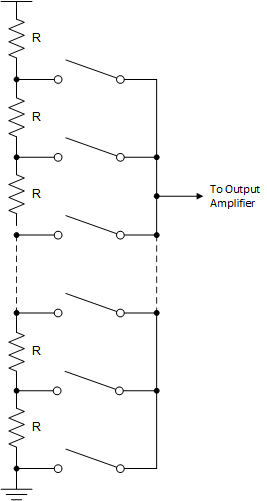
Figure 7-1 shows that the resistor string structure consists of a series of resistors, each of value R. The code loaded to the DAC determines the node on the string at which the voltage is tapped off to be fed into the output amplifier. The voltage is tapped off by closing one of the switches connecting the string to the amplifier. The resistor string architecture has inherent monotonicity, voltage output, and low glitch.
GUID-4B412528-0804-44CA-96F2-855F1AB927B0-low.gif Figure 7-1 DAC Resistor String