JAJSR83 September 2023 AMC131M02
PRODUCTION DATA
- 1
- 1 特長
- 2 アプリケーション
- 3 概要
- 4 Revision History
- 5 Pin Configuration and Functions
-
6 Specifications
- 6.1 Absolute Maximum Ratings
- 6.2 ESD Ratings
- 6.3 Recommended Operating Conditions
- 6.4 Thermal Information
- 6.5 Insulation Specifications
- 6.6 Safety-Related Certifications
- 6.7 Safety Limiting Values
- 6.8 Electrical Characteristics
- 6.9 Timing Requirements
- 6.10 Switching Characteristics
- 6.11 Timing Diagrams
- 6.12 Typical Characteristics
- 7 Parameter Measurement Information
-
8 Detailed Description
- 8.1 Overview
- 8.2 Functional Block Diagram
- 8.3
Feature Description
- 8.3.1 Isolated DC/DC Converter
- 8.3.2 High-Side Current Drive Capability
- 8.3.3 Isolation Channel Signal Transmission
- 8.3.4 Input ESD Protection Circuitry
- 8.3.5 Input Multiplexer
- 8.3.6 Programmable Gain Amplifier (PGA)
- 8.3.7 Voltage Reference
- 8.3.8 Internal Test Signals
- 8.3.9 Clocking and Power Modes
- 8.3.10 ΔΣ Modulator
- 8.3.11 Digital Filter
- 8.3.12 Channel Phase Calibration
- 8.3.13 Calibration Registers
- 8.3.14 Register Map CRC
- 8.3.15 General-Purpose Digital Output (GPO)
- 8.4 Device Functional Modes
- 8.5
Programming
- 8.5.1
Serial Interface
- 8.5.1.1 Chip Select (CS)
- 8.5.1.2 Serial Data Clock (SCLK)
- 8.5.1.3 Serial Data Input (DIN)
- 8.5.1.4 Serial Data Output (DOUT)
- 8.5.1.5 Data Ready (DRDY)
- 8.5.1.6 Conversion Synchronization or System Reset (SYNC/RESET)
- 8.5.1.7 SPI Communication Frames
- 8.5.1.8 SPI Communication Words
- 8.5.1.9 Short SPI Frames
- 8.5.1.10 Communication Cyclic Redundancy Check (CRC)
- 8.5.1.11 SPI Timeout
- 8.5.2 ADC Conversion Data
- 8.5.3 Commands
- 8.5.4 ADC Output Buffer and FIFO Buffer
- 8.5.5 Collecting Data for the First Time or After a Pause in Data Collection
- 8.5.1
Serial Interface
- 8.6 AMC131M02 Registers
- 9 Application and Implementation
- 10Device and Documentation Support
- 11Mechanical, Packaging, and Orderable Information
7.1 Noise Measurements
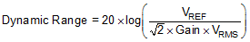
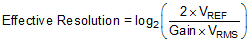
Adjust the data rate and gain to optimize the AMC131M02 noise performance. When averaging is increased by reducing the data rate, noise drops correspondingly. Table 7-1 summarizes the AMC131M02 noise performance using the 1.2-V internal reference and a 3.3-V power supply at the DVDD pin. Data are representative of typical noise performance at TA = 25°C when fCLKIN = 8.192 MHz. The clock divider is configured to the default setting (that is, the CLK_SEL[1:0] bits in the CLOCK register are set to 00b), thus the modulator clock frequency (fMOD) is equal to fCLKIN / 2. The data shown are typical input-referred noise results with the analog inputs shorted together and taking an average of multiple readings on channel 0. A minimum 1 second of consecutive readings are used to calculate the RMS noise for each reading. Table 7-2 lists the dynamic range, and Table 7-3 lists the effective resolution calculated from the noise data. Equation 1 calculates dynamic range. Equation 2 calculates effective resolution. In each case, VREF corresponds to the internal 1.2-V reference. In global-chop mode, noise improves by a factor of √2.
Noise performance scales with the OSR and gain settings, but is independent from the configured power mode. Thus, the device exhibits the same noise performance in different power modes when selecting the same OSR and gain settings. However, the data rate at the OSR settings scales based on the applied clock frequency for the different power modes.
| OSR | DATA RATE (kSPS), fCLKIN = 8.192 MHz |
GAIN | |||||||
|---|---|---|---|---|---|---|---|---|---|
| 1 | 2 | 4 | 8 | 16 | 32 | 64 | 128 | ||
| 16384 | 0.25 | 3.92 | 2.15 | 1.69 | 0.97 | 0.84 | 0.47 | 0.57 | 0.51 |
| 8192 | 0.5 | 4.55 | 3.16 | 2.91 | 2.23 | 1.67 | 1.55 | 1.07 | 0.92 |
| 4096 | 1 | 6.35 | 3.85 | 3.17 | 2.43 | 1.76 | 1.56 | 1.53 | 1.67 |
| 2048 | 2 | 7.55 | 4.92 | 3.92 | 2.94 | 2.46 | 1.68 | 1.56 | 1.85 |
| 1024 | 4 | 8.43 | 6.06 | 5.04 | 4.03 | 3.39 | 1.75 | 2.03 | 2.86 |
| 512 | 8 | 12.26 | 9.21 | 7.60 | 6.34 | 5.15 | 4.22 | 4.63 | 4.36 |
| 256 | 16 | 17.45 | 11.88 | 10.51 | 8.39 | 7.10 | 6.35 | 5.58 | 4.75 |
| 128 | 32 | 26.24 | 17.20 | 14.68 | 10.44 | 7.75 | 7.72 | 8.35 | 7.87 |
| 64 | 64 | 77.32 | 42.11 | 28.44 | 16.83 | 10.89 | 9.94 | 9.06 | 8.99 |
| OSR | DATA RATE (kSPS), fCLKIN = 8.192 MHz |
GAIN | |||||||
|---|---|---|---|---|---|---|---|---|---|
| 1 | 2 | 4 | 8 | 16 | 32 | 64 | 128 | ||
| 16384 | 0.25 | 107 | 106 | 102 | 101 | 96 | 95 | 87 | 82 |
| 8192 | 0.5 | 105 | 103 | 97 | 94 | 90 | 85 | 82 | 77 |
| 4096 | 1 | 103 | 101 | 97 | 93 | 90 | 85 | 79 | 72 |
| 2048 | 2 | 101 | 99 | 95 | 91 | 87 | 84 | 79 | 71 |
| 1024 | 4 | 100 | 97 | 92 | 88 | 84 | 84 | 76 | 67 |
| 512 | 8 | 97 | 93 | 89 | 84 | 80 | 76 | 69 | 64 |
| 256 | 16 | 94 | 91 | 86 | 82 | 77 | 72 | 68 | 63 |
| 128 | 32 | 90 | 88 | 83 | 80 | 77 | 71 | 64 | 59 |
| 64 | 64 | 81 | 80 | 77 | 76 | 74 | 69 | 63 | 57 |
| OSR | DATA RATE (kSPS), fCLKIN = 8.192 MHz |
GAIN | |||||||
|---|---|---|---|---|---|---|---|---|---|
| 1 | 2 | 4 | 8 | 16 | 32 | 64 | 128 | ||
| 16384 | 0.25 | 19.2 | 19.1 | 18.4 | 18.2 | 17.4 | 17.3 | 16.0 | 15.2 |
| 8192 | 0.5 | 19.0 | 18.5 | 17.7 | 17.0 | 16.5 | 15.6 | 15.1 | 14.3 |
| 4096 | 1 | 18.5 | 18.2 | 17.5 | 16.9 | 16.4 | 15.5 | 14.6 | 13.5 |
| 2048 | 2 | 18.3 | 17.9 | 17.2 | 16.6 | 15.9 | 15.4 | 14.6 | 13.3 |
| 1024 | 4 | 18.1 | 17.6 | 16.9 | 16.2 | 15.4 | 15.4 | 14.2 | 12.7 |
| 512 | 8 | 17.6 | 17.0 | 16.3 | 15.5 | 14.8 | 14.1 | 13.0 | 12.1 |
| 256 | 16 | 17.1 | 16.6 | 15.8 | 15.1 | 14.4 | 13.5 | 12.7 | 11.9 |
| 128 | 32 | 16.5 | 16.1 | 15.3 | 14.8 | 14.2 | 13.2 | 12.1 | 11.2 |
| 64 | 64 | 14.9 | 14.8 | 14.4 | 14.1 | 13.7 | 12.9 | 12.0 | 11.0 |