JAJSEW2D May 2017 – December 2021 AWR1243
PRODUCTION DATA
- 1 特長
- 2 アプリケーション
- 3 概要
- 4 Functional Block Diagram
- 5 Revision History
- 6 Device Comparison
- 7 Terminal Configuration and Functions
-
8 Specifications
- 8.1 Absolute Maximum Ratings
- 8.2 ESD Ratings
- 8.3 Power-On Hours (POH)
- 8.4 Recommended Operating Conditions
- 8.5 Power Supply Specifications
- 8.6 Power Consumption Summary
- 8.7 RF Specification
- 8.8 Thermal Resistance Characteristics for FCBGA Package [ABL0161]
- 8.9
Timing and Switching Characteristics
- 8.9.1 Power Supply Sequencing and Reset Timing
- 8.9.2 Synchronized Frame Triggering
- 8.9.3 Input Clocks and Oscillators
- 8.9.4 Multibuffered / Standard Serial Peripheral Interface (MibSPI)
- 8.9.5 LVDS Interface Configuration
- 8.9.6 General-Purpose Input/Output
- 8.9.7 Camera Serial Interface (CSI)
- 9 Detailed Description
- 10Monitoring and Diagnostics
- 11Applications, Implementation, and Layout
- 12Device and Documentation Support
- 13Mechanical, Packaging, and Orderable Information
パッケージ・オプション
デバイスごとのパッケージ図は、PDF版データシートをご参照ください。
メカニカル・データ(パッケージ|ピン)
- ABL|161
サーマルパッド・メカニカル・データ
発注情報
12.1 Device Nomenclature
To designate the stages in the product development cycle, TI assigns prefixes to the part numbers of all microprocessors (MPUs) and support tools. Each device has one of three prefixes: X, P, or null (no prefix) (for example, AWR1243). Texas Instruments recommends two of three possible prefix designators for its support tools: TMDX and TMDS. These prefixes represent evolutionary stages of product development from engineering prototypes (TMDX) through fully qualified production devices and tools (TMDS).
Device development evolutionary flow:
- XExperimental device that is not necessarily representative of the final device's electrical specifications and may not use production assembly flow.
- PPrototype device that is not necessarily the final silicon die and may not necessarily meet final electrical specifications.
- nullProduction version of the silicon die that is fully qualified.
Support tool development evolutionary flow:
- TMDXDevelopment-support product that has not yet completed Texas Instruments internal qualification testing.
- TMDSFully-qualified development-support product.
X and P devices and TMDX development-support tools are shipped against the following disclaimer:
"Developmental product is intended for internal evaluation purposes."
Production devices and TMDS development-support tools have been characterized fully, and the quality and reliability of the device have been demonstrated fully. TI's standard warranty applies.
Predictions show that prototype devices (X or P) have a greater failure rate than the standard production devices. Texas Instruments recommends that these devices not be used in any production system because their expected end-use failure rate still is undefined. Only qualified production devices are to be used.
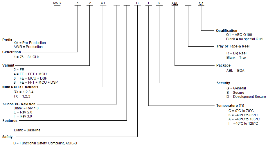
TI device nomenclature also includes a suffix with the device family name. This suffix indicates the package type (for example, ABL0161ALB0161), the temperature range (for example, blank is the default commercial temperature range). Figure 12-1 provides a legend for reading the complete device name for any AWR1243 device.
For orderable part numbers of AWR1243 devices in the ABL0161 package types, see the Package Option Addendum of this document , the TI website (www.ti.com), or contact your TI sales representative.
For additional description of the device nomenclature markings on the die, see the AWR1243 Device Errata .
 Figure 12-1 Device Nomenclature