JAJSGQ0G March 2013 – March 2019
PRODUCTION DATA.
- 1 特長
- 2 アプリケーション
- 3 概要
- 4 改訂履歴
- 5 Pin Configuration and Functions
- 6 Specifications
-
7 Detailed Description
- 7.1 Overview
- 7.2 Functional Block Diagram
- 7.3
Feature Description
- 7.3.1 Maximum Power Point Tracking
- 7.3.2 Battery Undervoltage Protection
- 7.3.3 Battery Overvoltage Protection
- 7.3.4 Battery Voltage within Operating Range (VBAT_OK Output)
- 7.3.5 Storage Element / Battery Management
- 7.3.6 Programming OUT Regulation Voltage
- 7.3.7 Step Down (Buck) Converter
- 7.3.8 Nano-Power Management and Efficiency
- 7.4 Device Functional Modes
- 8 Application and Implementation
- 9 Power Supply Recommendations
- 10Layout
- 11デバイスおよびドキュメントのサポート
- 12メカニカル、パッケージ、および注文情報
パッケージ・オプション
メカニカル・データ(パッケージ|ピン)
- RGR|20
サーマルパッド・メカニカル・データ
- RGR|20
発注情報
6.7 Typical Characteristics
Unless otherwise noted, graphs were taken using Figure 24 with CIN = 4.7µF, L1 = Coilcraft 22µH LPS4018, CSTOR = 4.7µF, L2 = Toko 10 µH DFE252012C, COUT = 22µF, VBAT_OV=4.2V, VOUT=1.8VTable 1. Table of Graphs
| FIGURE | |||
|---|---|---|---|
| Charger Efficiency (η)(1) | vs. Input Voltage | IN= 10 µA | Figure 1 |
| IN= 100 µA | Figure 2 | ||
| IIN = 10 mA | Figure 3 | ||
| vs. Input Current | VIN = 2.0 V | Figure 4 | |
| VIN = 1.0 V | Figure 5 | ||
| VIN = 0.5 V | Figure 6 | ||
| VIN = 0.2 V | Figure 7 | ||
| VSTOR Quiescent Current | vs. VSTOR Voltage | EN = 1, VOUT_EN = X (Ship Mode) | Figure 8 |
| EN = 0, VOUT_EN = 0 (Standby Mode) | Figure 9 | ||
| VBAT Quiescent Current | vs. VBAT Voltage | EN = 0, VOUT_EN = 1 (Active Mode) | Figure 10 |
| Buck Efficiency (η) | vs. Output Current | Figure 11 | |
| vs. Input Voltage | Figure 12 | ||
| Normalized Buck Output Voltage | vs. Output Current | Figure 13 | |
| vs. Input Voltage | Figure 14 | ||
| vs. Temperature | Figure 15 | ||
| Buck Maximum Output Current vs. Input Voltage | VOUT = 1.8V - 100mV | Figure 16 | |
| Buck Major Switching Frequency | vs. Output Current | Figure 17 | |
| vs. Input Voltage | Figure 18 | ||
| Buck Output Ripple | vs.Output Current | Figure 19 | |
| vs. Input Voltage | Figure 20 | ||
(1) See SLUA691 for an explanation on how to take these measurements. Because the MPPT feature cannot be disabled on the bq25570, these measurements need to be taken in the middle of the 16 s sampling period.
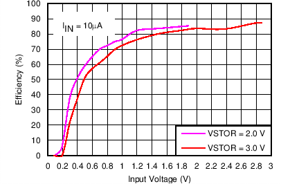
| VIN_DC = sourcemeter configured with ICOMP = 10 µA and outputing 0 to 3.0 V |
| VSTOR = sourcemeter configured to measure current and voltage source set to hold the VSTOR voltage = 2.0 V or 3.0 V |
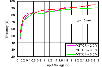
| VIN_DC = sourcemeter configured with ICOMP = 10 mA and voltage source varied from 0.1 V to 3.0 V |
| VSTOR = sourcemeter configured to measure current and voltage source set to hold the VSTOR voltage = 2.0 V, 3.0 V or 5.5 V |
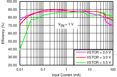
| VIN_DC = sourcemeter configured with voltage source = 1.0 V and ICOMP varied from 0.01 mA to 100 mA |
| VSTOR = sourcemeter configured to measure current and voltage source set to hold the VSTOR voltage = 2.0 V, 3.0 V or 5.5 V |
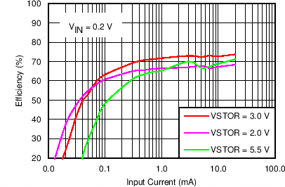
| VIN_DC = souremeter configured with voltage source = 0.2 V and ICOMP varied from 0.01 mA to 100 mA |
| VSTOR = sourcemeter configured to measure current and voltage source set to hold the VSTOR voltage = 2.0 V, 3.0 V or 5.5 V |
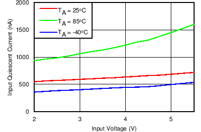
| VIN_DC = floating and EN = GND and VOUT_EN=VSTOR |
| VSTOR= sourcemeter configured to measure current and voltage source varied from 2.0 V or 5.5 V |
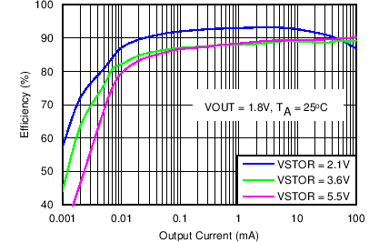
| VSTOR = sourcemeter configured as a voltage source, measuring current | ||
| OUT = sourcemeter configured to sink current with VCOMP>V(OUT) |
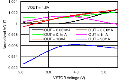
| VSTOR = sourcemeter configured as a voltage source | ||
| OUT = sourcemeter configured to sink current with VCOMP>V(OUT) and measuring voltage |
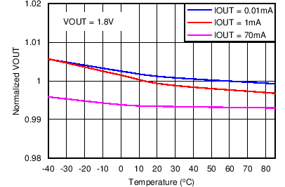
| VSTOR = sourcemeter configured as a voltage source | ||
| OUT = sourcemeter configured to sink current with VCOMP>V(OUT) and measuring voltage | ||
| Thermal stream for temperature variation |
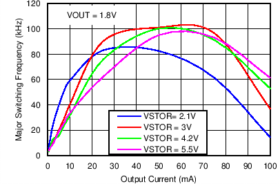
| VSTOR = sourcemeter configured as a voltage source | ||
| OUT = sourcemeter configured to sink current with VCOMP>V(OUT) and measuring voltage | ||
| Oscilloscope used to measure switching frequency at LBOOST |
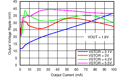
| VSTOR = sourcemeter configured as a voltage source | ||
| OUT = sourcemeter configured to sink current with VCOMP>V(OUT) and measuring voltage | ||
| Oscilloscope used to measure voltage ripple at OUT |
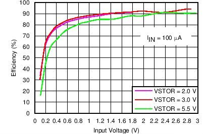
| VIN_DC = Keithley Source Meter configured with ICOMP = 100 µA and voltage source varied from 0.1 V to 3.0 V s | ||
| VSTOR = Keithley Sourcemeter configured to measure current and voltage source set to hold the VSTOR voltage = 2.0 V, 3.0 V or 5.5 V |
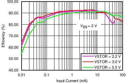
| VIN_DC = sourcemeter configured with voltage source = 2.0 V and ICOMP varied from 0.01 mA to 100 mA |
| VSTOR = sourcemeter configured to measure current and voltage source set to hold the VSTOR voltage = 2.2 V , 3.0 V or 5.5 V |
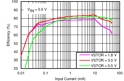
| VIN_DC = sourcemeter configured with voltage source = 0.5 V and ICOMP varied from 0.01 mA to 100 mA |
| VSTOR = sourcemeter configured to measure current and voltage source set to hold the VSTOR voltage = 1.8 V, 3.0 V or 5.5 V |
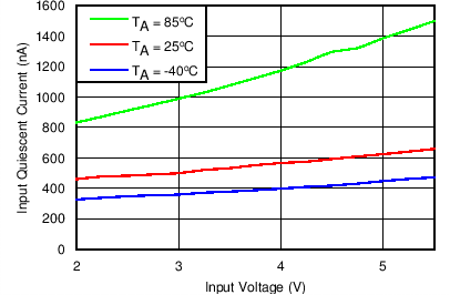
| VIN_DC = floating and EN = VOUT_EN = GND |
| VSTOR = sourcemeter configured to measure current and voltage source varied from 2.0 V or 5.5 V |
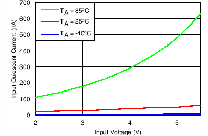
| VIN_DC = floating and EN = VSTOR |
| VSTOR = sourcemeter configured to measure current and voltage source varied from 2.0 V or 5.5 V |
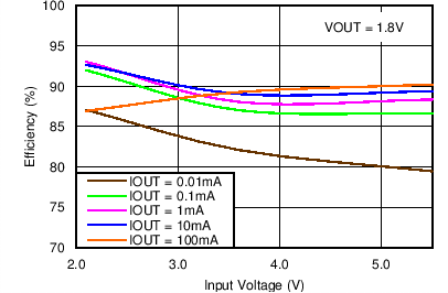
| VSTOR = sourcemeter configured as a voltage source, measuring current | ||
| OUT = sourcemeter configured sink current with VCOMP>V(OUT) | ||
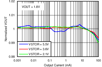
| VSTOR = sourcemeter configured as a voltage source | ||
| OUT = sourcemeter configured to sink current with VCOMP>V(OUT) and measuring voltage |
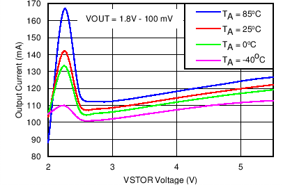
| VSTOR = sourcemeter configured as a voltage source | ||
| OUT = sourcemeter configured to increasingly sink current with VCOMP>V(OUT) until V(OUT) < VOUT - 100 mV | ||
| Thermal stream for temperature variation |
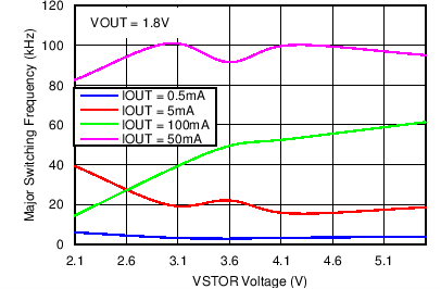
| VSTOR = sourcemeter configured as a voltage source | ||
| OUT = sourcemeter configured to sink current with VCOMP>V(OUT) and measuring voltage | ||
| Oscilloscope used to measure switching frequency at LBOOST |
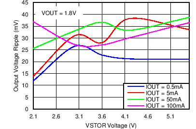
| VSTOR = sourcemeter configured as a voltage source | ||
| OUT = sourcemeter configured to sink current with VCOMP>V(OUT) and measuring voltage | ||
| Oscilloscope used to measure voltage ripple at OUT |