JAJSGQ0G March   2013  – March 2019

PRODUCTION DATA.  

  1. 特長
  2. アプリケーション
  3. 概要
    1.     Device Images
      1.      代表的なアプリケーション回路図
      2.      充電器の効率と入力電圧との関係
  4. 改訂履歴
  5. Pin Configuration and Functions
    1.     Pin Functions
  6. Specifications
    1. 6.1 Absolute Maximum Ratings
    2. 6.2 ESD Ratings
    3. 6.3 Recommended Operating Conditions
    4. 6.4 Thermal Information
    5. 6.5 Electrical Characteristics
    6. 6.6 Electrical Characteristics
    7. 6.7 Typical Characteristics
  7. Detailed Description
    1. 7.1 Overview
    2. 7.2 Functional Block Diagram
    3. 7.3 Feature Description
      1. 7.3.1 Maximum Power Point Tracking
      2. 7.3.2 Battery Undervoltage Protection
      3. 7.3.3 Battery Overvoltage Protection
      4. 7.3.4 Battery Voltage within Operating Range (VBAT_OK Output)
      5. 7.3.5 Storage Element / Battery Management
      6. 7.3.6 Programming OUT Regulation Voltage
      7. 7.3.7 Step Down (Buck) Converter
      8. 7.3.8 Nano-Power Management and Efficiency
    4. 7.4 Device Functional Modes
      1. 7.4.1 Main Boost Charger Disabled (Ship Mode) - (VSTOR > VSTOR_CHGEN and EN = HIGH)
      2. 7.4.2 Cold-Start Operation (VSTOR < VSTOR_CHGEN, VIN_DC > VIN(CS) and PIN > PIN(CS), EN = don't care)
      3. 7.4.3 Main Boost Charger Enabled (VSTOR > VSTOR_CHGEN and EN = LOW )
        1. 7.4.3.1 Buck Converter Enabled (VSTOR > VBAT_UV, EN = LOW and VOUT_EN = HIGH )
      4. 7.4.4 Thermal Shutdown
  8. Application and Implementation
    1. 8.1 Application Information
      1. 8.1.1 Energy Harvester Selection
      2. 8.1.2 Storage Element Selection
      3. 8.1.3 Inductor Selection
        1. 8.1.3.1 Boost Charger Inductor Selection
        2. 8.1.3.2 Buck Converter Inductor Selection
      4. 8.1.4 Capacitor Selection
        1. 8.1.4.1 VREF_SAMP Capacitance
        2. 8.1.4.2 VIN_DC Capacitance
        3. 8.1.4.3 VSTOR Capacitance
        4. 8.1.4.4 VOUT Capacitance
        5. 8.1.4.5 Additional Capacitance on VSTOR or VBAT
    2. 8.2 Typical Applications
      1. 8.2.1 Solar Application Circuit
        1. 8.2.1.1 Design Requirements
        2. 8.2.1.2 Detailed Design Procedure
        3. 8.2.1.3 Application Curves
      2. 8.2.2 TEG Application Circuit
        1. 8.2.2.1 Design Requirements
        2. 8.2.2.2 Detailed Design Procedure
        3. 8.2.2.3 Application Curves
      3. 8.2.3 Piezoelectric Application Circuit
        1. 8.2.3.1 Design Requirements
        2. 8.2.3.2 Detailed Design Procedure
        3. 8.2.3.3 Application Curves
  9. Power Supply Recommendations
  10. 10Layout
    1. 10.1 Layout Guidelines
    2. 10.2 Layout Example
    3. 10.3 Thermal Considerations
  11. 11デバイスおよびドキュメントのサポート
    1. 11.1 デバイス・サポート
      1. 11.1.1 デベロッパー・ネットワークの製品に関する免責事項
    2. 11.2 ドキュメントのサポート
      1. 11.2.1 関連資料
    3. 11.3 ドキュメントの更新通知を受け取る方法
    4. 11.4 コミュニティ・リソース
    5. 11.5 商標
    6. 11.6 静電気放電に関する注意事項
    7. 11.7 Glossary
  12. 12メカニカル、パッケージ、および注文情報

パッケージ・オプション

メカニカル・データ(パッケージ|ピン)
サーマルパッド・メカニカル・データ
発注情報

Application Curves

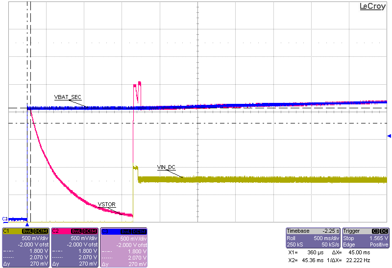
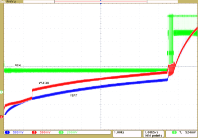
bq25570 app1_startup_1VIN_8p5ma_100kohm_slusbj3.png
Sourcemeter with VSOURCE = 1.0 V and compliance of 8.5 mA subsequently applied to VIN_DC
VBAT = 0.1 F capacitor charged to 2.0 V
Resistance on VSTOR = 100 kΩ
Figure 25. Startup by Battery Attach With Almost Depleted Storage Element
bq25570 app1_mppt_ov_4p2v_3vstor_2p0vin_42p6ma_slusbj3.png
VIN_DC = sourcemeter with VSOURCE = 2.0 V and compliance
of 43 mA
VBAT = sourcemeter with VSOURCE = 3.0 V and compliance
of 1 A
Figure 27. MPPT Operation
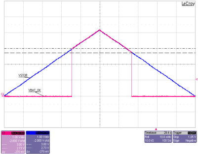
bq25570 bq25570_bq25505-vbat-ok1_lusbh2.gif
VIN_DC = 1.5 V with 75 Ω series resistance
No storage element on VBAT or VBAT_PRI
VSTOR artifically ramped from 0 V to 4.2 V to 0 V using a power amp driven by a function generator
Figure 29. VBAT_OK Operation
bq25570 bq25505-ds21_50MA-LD_TRN.png
VIN_DC = 1.5 V with 75 Ω series resistance
VBAT = 4.2 V charged 0.5 F capacitor
R(VSTOR) = open to 84 Ω to open
Figure 31. 50 mA Load Transient on VSTOR - Zoom Out
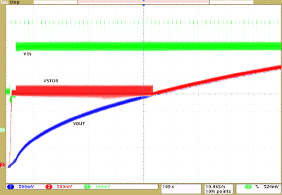
bq25570 supercap_VOUT_lusbh2.gif
VIN_DC = source meter with 1.2 V compliance and ISC = 1.0 mA
120 mF super capacitor on VOUT with VOUT regulation voltage changed to 4.2 V.
Figure 33. Charging a Super Capacitor on VOUT
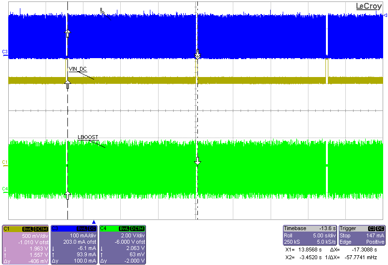
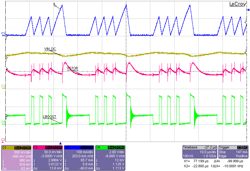
bq25570 app2_operation_ov_5p0v_3vstor_2p0vin_42p6ma_slusbj3.png
VIN_DC = sourcemeter with VSOURCE = 2.0 V and compliance of 43 mA
VBAT = sourcemeter with VSOURCE = 3.0 V and compliance of
1 A
IL = inductor current
Figure 26. Boost Charger Operational Waveforms
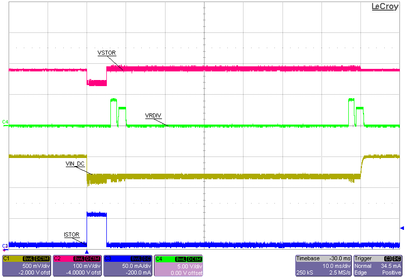
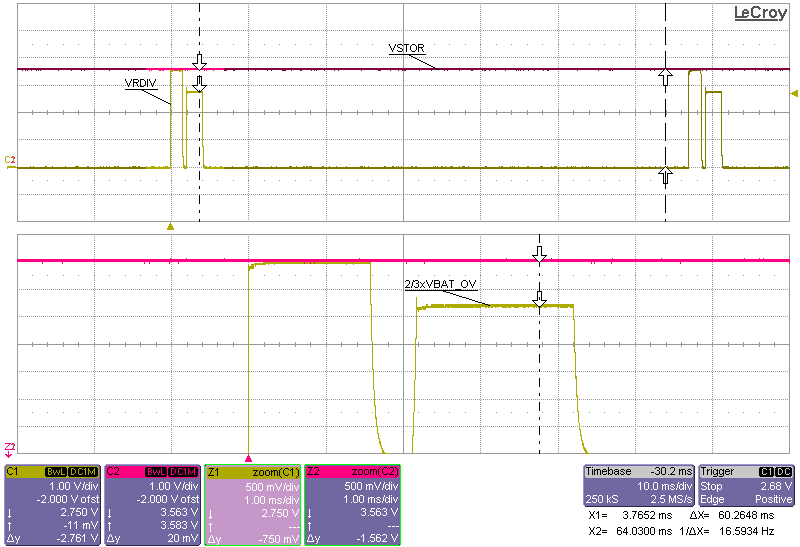
bq25570 app1_VRDIV_ov_4p2v_slusbj3.png
VIN_DC = sourcemeter with VSOURCE = 2.0 V and compliance of 43 mA
VBAT = sourcemeter with VSOURCE = 3.6 V and compliance
of 1 A
Figure 28. VRDIV Waveform
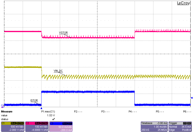
bq25570 bq25505-ds20-50MA-LD_TRN.png
VIN_DC = 1.5 V with 75 Ω series resistance
VBAT = 4.2 V charged 0.5 F capacitor
R(VSTOR) = open to 84 Ω to open
Figure 30. 50 mA Load Transient on VSTOR
bq25570 supercap_VBAT_lusbh2.gif
VIN_DC = source meter with 1.2 V compliance and ISC = 1.0 mA
120 mF super capacitor on VBAT
Figure 32. Charging a Super Capacitor on VBAT