JAJSS91 November 2023 BQ25756E
PRODUCTION DATA
- 1
- 1 特長
- 2 アプリケーション
- 3 概要
- 4 概要 (続き)
- 5 Device Comparison
- 6 Pin Configuration and Functions
- 7 Specifications
-
8 Detailed Description
- 8.1 Overview
- 8.2 Functional Block Diagram
- 8.3
Feature Description
- 8.3.1 Device Power-On-Reset
- 8.3.2 Device Power-Up From Battery Without Input Source
- 8.3.3 Device Power Up from Input Source
- 8.3.4 Battery Charging Management
- 8.3.5 Power Management
- 8.3.6 Reverse Mode Power Direction
- 8.3.7 Integrated 16-Bit ADC for Monitoring
- 8.3.8 Status Outputs (PG, STAT1, STAT2, and INT)
- 8.3.9
Protections
- 8.3.9.1
Voltage and Current Monitoring
- 8.3.9.1.1 VAC Over-voltage Protection (VAC_OVP)
- 8.3.9.1.2 VAC Under-voltage Protection (VAC_UVP)
- 8.3.9.1.3 Battery Over-voltage Protection (BAT_OVP)
- 8.3.9.1.4 Battery Over-current Protection (BAT_OCP)
- 8.3.9.1.5 Reverse Mode Over-voltage Protection (REV_OVP)
- 8.3.9.1.6 Reverse Mode Under-voltage Protection (REV_UVP)
- 8.3.9.1.7 DRV_SUP Under-voltage and Over-voltage Protection (DRV_OKZ)
- 8.3.9.1.8 REGN Under-voltage Protection (REGN_OKZ)
- 8.3.9.2 Thermal Shutdown (TSHUT)
- 8.3.9.1
Voltage and Current Monitoring
- 8.3.10 Serial Interface
- 8.4 Device Functional Modes
- 8.5 BQ25756E Registers
-
9 Application and Implementation
- 9.1 Application Information
- 9.2
Typical Applications
- 9.2.1
Typical Application
- 9.2.1.1 Design Requirements
- 9.2.1.2
Detailed Design Procedure
- 9.2.1.2.1 ACUV / ACOV Input Voltage Operating Window Programming
- 9.2.1.2.2 Charge Voltage Selection
- 9.2.1.2.3 Switching Frequency Selection
- 9.2.1.2.4 Inductor Selection
- 9.2.1.2.5 Input (VAC) Capacitor
- 9.2.1.2.6 Output (VBAT) Capacitor
- 9.2.1.2.7 Sense Resistor (RAC_SNS and RBAT_SNS) and Current Programming
- 9.2.1.2.8 Power MOSFETs Selection
- 9.2.1.2.9 Converter Fast Transient Response
- 9.2.1.3 Application Curves
- 9.2.2 Typical Application (USB-PD EPR Configuration)
- 9.2.1
Typical Application
- 10Power Supply Recommendations
- 11Layout
- 12Device and Documentation Support
- 13Revision History
- 14Mechanical, Packaging, and Orderable Information
パッケージ・オプション
メカニカル・データ(パッケージ|ピン)
- RRV|36
サーマルパッド・メカニカル・データ
- RRV|36
発注情報
9.2.1.2.8 Power MOSFETs Selection
Four external N-channel MOSFETs are used for a synchronous switching buck-boost battery charger. The gate drivers are integrated into the IC with 5 V of gate drive voltage. An external gate drive voltage can be provided directly into the DRV_SUP pin for increased efficiency.
Figure-of-merit (FOM) is usually used for selecting proper MOSFET based on a tradeoff between the conduction loss and switching loss. For the top side MOSFET, FOM is defined as the product of a MOSFET's on-resistance, RDS(ON), and the gate-to-drain charge, QGD. For the bottom side MOSFET, FOM is defined as the product of the MOSFET's on-resistance, RDS(ON), and the total gate charge, QG.
The lower the FOM value, the lower the total power loss. Usually lower RDS(ON) has higher cost with the same package size.
The top-side MOSFET loss includes conduction loss and switching loss. Taking buck mode operation as an example the power loss is a function of duty cycle (D=VOUT/VIN), charging current (ICHG), MOSFET's on-resistance (RDS(ON)_top), input voltage (VIN), switching frequency (fS), turn-on time (ton) and turn-off time (toff):
- IL_DC is the average inductor DC current;
- Iripple is the inductor current ripple peak-to-peak value;
The first item Pcon_top represents the conduction loss which is straight forward. The second term Psw_top represents the multiple switching loss items in top MOSFET including voltage and current overlap losses (PIV_top), MOSFET parasitic output capacitance loss (PQoss_top) and gate drive loss (PGate_top). To calculate voltage and current overlap losses (PIV_top):
- ton is the MOSFET turn-on time that VDS falling time from VIN to almost zero (MOSFET turn on conduction voltage);
- toff is the MOSFET turn-off time that IDS falling time from Ipeak to zero;
The MOSFET turn-on and turn-off times are given by:
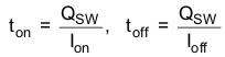
where Qsw is the switching charge, Ion is the turn-on gate driving current, and Ioff is the turn-off gate driving current. If the switching charge is not given in MOSFET datasheet, it can be estimated by gate-to-drain charge (QGD) and gate-to-source charge (QGS):
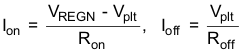
Gate driving current can be estimated by REGN voltage (VREGN), MOSFET plateau voltage (Vplt), total turn-on gate resistance (Ron), and turn-off gate resistance (Roff) of the gate driver:
To calculate top MOSFET parasitic output capacitance loss (PQoss_top):
- Qoss is the MOSFET parasitic output charge which can be found in MOSFET datasheet. It is recommended to limit the total switch node capacitance CSW (nF) < 160/VIN; for example, for a 36-V application, it is recommended to keep the total CSW < 4.44 nF
To calculate top MOSFET gate drive loss (PGate_top):
- QGate_top is the top MOSFET gate charge which can be found in MOSFET datasheet;
- Note here VIN is used instead of real gate drive voltage because the gate drive is generated based on LDO from VIN, the total gate drive related loss are all considered when VIN is used for gate drive loss calculation.
- Alternatively, gate drive voltage can be supplied directly by external high efficiency supply into the DRV_SUP pin. In this case, the power loss to drive the gates becomes: PGate_top =VDRV_SUP· QGate_top · fS
The bottom-side MOSFET loss also includes conduction loss and switching loss:
The first item Pcon_bottom represents the conduction loss which is straight forward. The second term Psw_bottom represents the multiple switching loss items in bottom MOSFET including reverse recovery losses (PRR_bottom), Dead time body diode conduction loss (PDead_bottom) and gate drive loss (PGate_bottom). The detail calculation can be found below:
- Qrr is the bottom MOSFET reverse recovery charge which can be found in MOSFET data sheet;
- VF is the body diode forward conduction voltage drop;
- tdead_rise is the SW rising edge deadtime between top and bottom MOSFETs which is around 45 ns;
- tdead_fall is the SW falling edge deadtime between top and bottom MOSFETs which is around 45 ns;
PGate_bottom can follow the same method as top MOSFET gate drive loss calculation approach.