JAJSL52A april 2020 – february 2021 BQ25968
PRODUCTION DATA
- 1
- 1 特長
- 2 アプリケーション
- 3 概要
- 4 Revision History
- 5 概要 (続き)
- 6 Device Comparison Table
- 7 Pin Configuration and Functions
- 8 Specifications
-
9 Detailed Description
- 9.1 Overview
- 9.2 Functional Block Diagram
- 9.3
Feature Description
- 9.3.1 Charging System
- 9.3.2 Battery Charging Profile
- 9.3.3 Control State Diagram for System Implementation
- 9.3.4 Device Power Up
- 9.3.5 Switched Cap Function
- 9.3.6 Charging Start-Up
- 9.3.7 Integrated 16-Bit ADC for Monitoring and Smart Adapter Feedback
- 9.3.8 Device Internal Thermal Shutdown, TSBUS, and TSBAT Temperature Monitoring
- 9.3.9 INT Pin, STAT, FLAG, and MASK Registers
- 9.3.10 CDRVH and CDRVL_ADDRMS Functions
- 9.3.11 Parallel Operation Using Master and Slave Modes
- 9.4 Device Functional Modes
- 9.5 Programming
- 9.6 Register Maps
- 10Application and Implementation
- 11Power Supply Recommendations
- 12Layout
- 13Device and Documentation Support
- 14Mechanical, Packaging, and Orderable Information
9.3.3 Control State Diagram for System Implementation
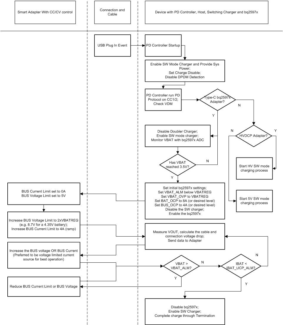
The device being charged will need to communicate with the adapter to control the current being delivered to the BQ25968. This is accomplished by using the adjustable protection and alarm settings in the BQ25968, and communicating to the wall charger (or power bank or car charge adapter) as shown in Figure 9-3. The availability of the alarms are dependant on the presence of the input supply and the charge state, which is shown in Table 9-1.
 Figure 9-3 System Control State
Diagram
Figure 9-3 System Control State
DiagramTable 9-1 ALM/FLT Function Activity
| ALM/FLT FUNCTION | BATTERY ONLY | VAC PRESENT CHG_EN = 0 | VAC PRESENT CHG_EN = 1 |
|---|---|---|---|
| BAT_OVP_ALM | Not Active | Not Active | Active |
| BAT_OCP_ALM | Not Active | Not Active | Active |
| BAT_UCP_ALM | Not Active | Not Active | Active |
| BUS_OVP_ALM | Not Active | Not Active | Active |
| BUS_OCP_ALM | Not Active | Not Active | Active |
| TSBUS_FLT | Not Active | Active | Active |
| TSBAT_FLT | Not Active | Active | Active |
| TDIE_ALM | Not Active | Active | Active |
| TSBUS_TSBAT_ALM | Not Active | Active | Active |