SLUSA92D January 2011 – May 2015
PRODUCTION DATA.
- 1 Features
- 2 Applications
- 3 Description
- 4 Simplified Schematic
- 5 Revision History
- 6 Pin Configuration and Functions
-
7 Specifications
- 7.1 Absolute Maximum Ratings
- 7.2 ESD Ratings
- 7.3 Recommended Operating Conditions
- 7.4 Thermal Information
- 7.5 Supply Current
- 7.6 Power-On Reset (POR)
- 7.7 WAKE FROM SLEEP
- 7.8 RBI RAM Backup
- 7.9 3.3-V Regulator
- 7.10 2.5-V Regulator
- 7.11 DISP, PRES, SMBD, SMBC
- 7.12 CHG, DSG FET Drive
- 7.13 Internal Precharge Limiting
- 7.14 GPOD
- 7.15 FUSE
- 7.16 LED5, LED4, LED3, LED2, LED1
- 7.17 Coulomb Counter
- 7.18 VC1, VC2, VC3, VC4
- 7.19 TS1, TS2
- 7.20 Internal Temperature Sensor
- 7.21 Internal Thermal Shutdown
- 7.22 High Frequency Oscillator
- 7.23 Low Frequency Oscillator
- 7.24 Internal Voltage Reference
- 7.25 Flash
- 7.26 OCD Current Protection
- 7.27 SCD1 Current Protection
- 7.28 SCD2 Current Protection
- 7.29 SCC Current Protection
- 7.30 SBS Timing Requirements
- 7.31 Typical Characteristics
- 8 Detailed Description
- 9 Application and Implementation
- 10Power Supply Recommendations
- 11Layout
- 12Device and Documentation Support
- 13Mechanical, Packaging, and Orderable Information
9 Application and Implementation
NOTE
Information in the following applications sections is not part of the TI component specification, and TI does not warrant its accuracy or completeness. TI’s customers are responsible for determining suitability of components for their purposes. Customers should validate and test their design implementation to confirm system functionality.
9.1 Application Information
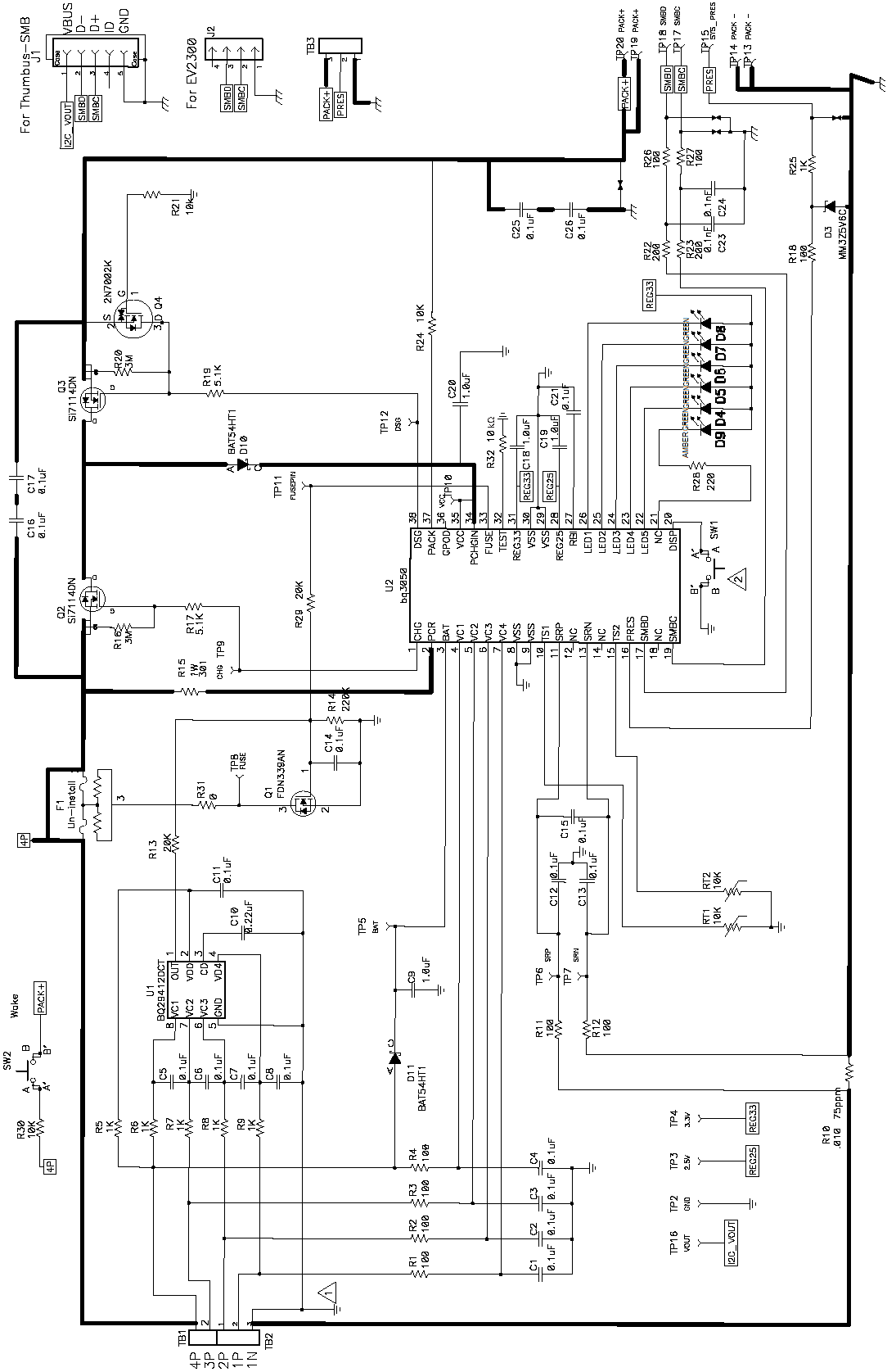
The bq3050 gas gauge is a primary protection device that can be used with a 2-series, 3-series or 4-series Li-Ion/Li Polymer battery pack. To implement and design a comprehensive set of parameters for a specific battery pack, the user needs the bqEVSW tool, which is a graphical user-interface tool installed on a PC during development. The firmware installed in the product has default values, which are summarized in the bq3050 Technical Reference Manual(SLUU485). Using the bqEVSW tool, these default values can be changed to cater to specific application requirements during development once the system parameters are known, such as fault-trigger thresholds for protection, enable or disable certain features for operation, configuration of cells, and more.
9.2 Typical Applications
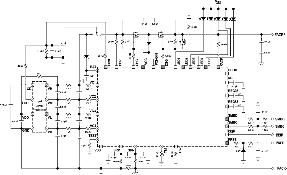
In a typical application, the bq3050 is typically paired with a 2nd-level overvoltage protection device to provide an independent level of voltage protection.
The bq3050 is often used to provide a visual display using the LED Display feature, but this is optional.
9.2.1 Design Requirements
For the bq3050 design example, use the parameters in Table 1 as input parameters.
Table 1. Requirements
| DESIGN PARAMETER | VALUE OR STATE |
|---|---|
| Cell Configuration | 3s2p (4-series with 1 Parallel) |
| Design Capacity | 4400 mAh |
| Device Chemistry | Chem ID 100 (LiCoO2/graphitized carbon) |
| Cell Overvoltage (per cell) | 4500 mV |
| Cell Undervoltage (per cell) | 2200 mV |
| 1st Tier Overcurrent in CHARGE Mode | 6000 mA |
| 1st Tier Overcurrent in DISCHARGE Mode | –6000 mA |
| AFE Overcurrent in CHARGE Mode | 0.120 V/Rsense across SRP, SRN |
| AFE Short Circuit in DISCHARGE Mode | 0.450 V/Rsense across SRP, SRN |
| AFE Short Circuit in CHARGE Mode | 0.250V/Rsense across SRP, SRN |
| Overtemperature in CHARGE Mode | 55°C |
| Overtemperature in DISCHARGE Mode | 60°C |
| SAFE Pin Activation Enabled | No |
| Safety Overvoltage (per cell) | 4600 mV |
| Shutdown Voltage | 5250 mV |
| Cell Balancing Enabled | Yes |
| Internal or External Temperature Sensor | External Enabled |
| SMB BROADCAST Mode | Disabled |
| Display Mode (Number of LEDs) | 5-bar |
| PRES Feature Enabled | No |
9.2.2 Detailed Design Procedure
9.2.2.1 High-Current Path
The high-current path begins at the PACK+ terminal of the battery pack. As charge current travels through the pack, it finds its way through protection FETs, a chemical fuse, the lithium-ion cells and cell connections, and the sense resistor, and then returns to the PACK– terminal (see ). In addition, some components are placed across the PACK+ and PACK– terminals to reduce effects from electrostatic discharge.
9.2.2.1.1 Protection FETs
The N-channel charge and discharge FETs must be selected for a given application (Figure 8). Most portable battery applications are a good match for the CSD17308Q3. The TI CSD17308Q3 is an 47A-A, 30-V device with Rds(on) of 8.2 mΩ when the gate drive voltage is 10 V.
If a precharge FET is used, R15 is calculated to limit the precharge current to the desired rate. Be sure to account for the power dissipation of the series resistor. The precharge current is limited to (Vcharger – Vbat)/R15 and maximum power dissipation is (Vcharger – Vbat)2/R15.
The gates of all protection FETs are pulled to the source with a high-value resistor between the gate and source to ensure they are turned off if the gate drive is open.
Capacitors C16 and C17 help protect the FETs during an ESD event. The use of two devices ensures normal operation if one of them becomes shorted. In order to have good ESD protection, the copper trace inductance of the capacitor leads must be designed to be as short and wide as possible. Ensure that the voltage rating of both C16 and C17 are adequate to hold off the applied voltage if one of the capacitors becomes shorted.
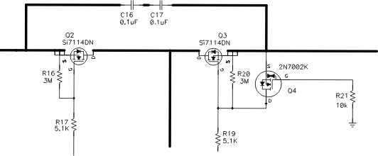 Figure 8. bq3050 Protection FETs
9.2.2.1.2 Chemical Fuse
The chemical fuse (Sony Chemical, Uchihashi, and so forth) is ignited under command from either the bq294705 secondary voltage protection IC or from the FUSE pin of the gas gauge. Either event applies a positive voltage to the gate of Q1, shown in Figure 9, which then sinks current from the third terminal of the fuse, causing it to ignite and open permanently.
It is important to carefully review the fuse specifications and match the required ignition current to that available from the N-channel FET. Ensure that the proper voltage, current, and Rds(on) ratings are used for this device. The fuse control circuit is discussed in detail in FUSE Circuitry.
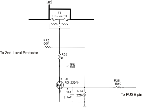 Figure 9. FUSE Circuit
9.2.2.1.3 Lithium-Ion Cell Connections
The important thing to remember about the cell connections is that high current flows through the top and bottom connections; therefore, the voltage sense leads at these points must be made with a Kelvin connection to avoid any errors due to a drop in the high-current copper trace. The location marked 4P in Figure 10 indicates the Kelvin connection of the most positive battery node. The connection marked 1N is equally important. The VC5 pin (a ground reference for cell voltage measurement), which is in the older generation devices, is not in the bq3050 device. Hence, the single-point connection at 1N to the low-current ground is needed to avoid an undesired voltage drop through long traces while the gas gauge is measuring the bottom cell voltage.
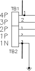 Figure 10. Lithium-Ion Cell Connections
9.2.2.1.4 Sense Resistor
As with the cell connections, the quality of the Kelvin connections at the sense resistor is critical. The sense resistor must have a temperature coefficient no greater than 75 ppm in order to minimize current measurement drift with temperature (Figure 11). Choose the value of the sense resistor to correspond to the available overcurrent and short-circuit ranges of the bq3050. Select the smallest value possible in order to minimize the negative voltage generated on the bq3050 VSS node(s) during a short circuit. This pin has an absolute minimum of –0.3 V. For a pack with two parallel cylindrical cells, 10 mΩ is generally ideal. Parallel resistors can be used as long as good Kelvin sensing is ensured.
The ground scheme of bq3050 is different from the older generation devices. In previous devices, the device ground (or low-current ground) is connected to the SRN side of the Rsense resistor pad. The bq3050, however, connects the low-current ground on the SRP side of the Rsense resistor pad, close to the battery 1N terminal (see Lithium-Ion Cell Connections). This is because the bq3050 has one less VC pin (a ground reference pin VC5) compared to the previous devices. The pin was removed and was internally combined to SRP.
 Figure 11. Sense Resistor
9.2.2.1.5 ESD Mitigation
A pair of series 0.1-μF ceramic capacitors is placed across the PACK+ and PACK– terminals to help in the mitigation of external electrostatic discharges. The two devices in series ensure continued operation of the pack if one of the capacitors becomes shorted.
Optionally, a tranzorb, such as the SMBJ2A, can be placed across the terminals to further improve ESD immunity.
9.2.2.2 Gas Gauge Circuit
The Gas Gauge Circuit includes the bq3050 and its peripheral components. These components are divided into the following groups: Differential Low-Pass Filter, Power Supply Decoupling/RBI, System Present, SMBus Communication, FUSE circuit, and LED.
9.2.2.2.1 Differential Low-Pass Filter
As shown in Figure 12, a differential filter must precede the current sense inputs of the gas gauge. This filter eliminates the effect of unwanted digital noise, which can cause offset in the measured current. Even the best differential amplifier has less common-mode rejection at high frequencies. Without a filter, the amplifier input stage may rectify a strong RF signal, which then may appear as a dc offset error.
Five percent tolerance of the components is adequate because capacitor C15 shunts C12/C13, and reduces AC common mode arising from component mismatch. It is also proven to reduce offset and noise error by maintaining µa symmetrical placement pattern and adding ground shielding for the differential filter network.
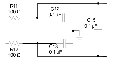 Figure 12. Differential Low-Pass Filter
9.2.2.2.2 Power Supply Decoupling and RBI
Power supply decoupling is important for optimal operation of the bq3050 advanced gas gauges. As shown in , a single 1.0-μF ceramic decoupling capacitor from REG33 to VSS and REG25 to VSS must be placed adjacent to the IC pins.
The RBI pin is used to supply backup RAM voltage during brief transient power outages. The partial reset mechanism makes use of the RAM to restore the critical CPU registers following a temporary loss of power. A standard 0.1-μF ceramic capacitor is connected from the RBI pin to ground, as shown in Figure 13.
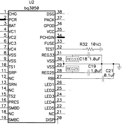 Figure 13. Power Supply Decoupling
9.2.2.2.3 System Present
The System Present signal is used to inform the gas gauge whether the pack is installed into or removed from the system. In the host system, this pin is grounded. The PRES pin of the bq3050 is occasionally sampled to test for system present. To save power, an internal pullup resistor is provided by the gas gauge during a brief 4-μs sampling pulse once per second.
Because the System Present signal is part of the pack connector interface to the outside world, it must be protected from external electrostatic discharge events. An integrated ESD protection on the PRES device pin reduces the external protection requirement to just R25 for an 8-kV ESD contact rating (Figure 14). However, if it is possible that the System Present signal may short to PACK+, then R18 and D3 must be included for high-voltage protection.
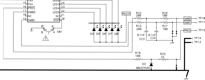 Figure 14. System Present ESD and Short Protection
9.2.2.2.4 SMBus Communication
Similar to the System Present pin, the SMBus clock and data pins have integrated high-voltage ESD protection circuits that reduce the need for external Zener diode protection. When using the circuit shown in Figure 15, the communication lines can withstand an 8-kV (contact) ESD strike. C23 and C24 are selected with a 100-pF value in order to meet the SMBus specifications. If it is desirable to provide increased protection with a larger input resistor and/or Zener diode, carefully investigate the signal quality of the SMBus signals under worst-case communication conditions.
The SMbus clock and data lines have internal pulldowns. When the gas gauge senses that both lines are low (such as during removal of the pack), the device performs auto-offset calibration and then goes into sleep mode to conserve power.
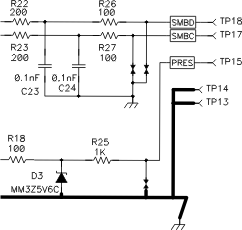 Figure 15. ESD Protection for SMB Communication
9.2.2.2.5 FUSE Circuitry
The FUSE pin of the bq3050 is designed to ignite the chemical fuse if one of the various safety criteria is violated (Figure 16). The FUSE pin also monitors the state of the secondary-voltage protection IC. Q3 ignites the chemical fuse when its gate is high. The 7-V output of the bq29705 is divided by R13 and R14, which provides adequate gate drive for Q1 while guarding against excessive back current into the bq29705 if the FUSE signal is high.
Using C14 is generally a good practice, especially for RFI immunity. C14 may be removed, if desired, because the chemical fuse is a comparatively slow device and is not affected by any sub-microsecond glitches that may come from the SAFE output during the cell connection process.
 Figure 16. FUSE Circuit
When the bq3050 is commanded to ignite the chemical fuse, the FUSE pin activates to give a typical 8-V output. The new design makes it possible to use a higher Vgs FET for Q1. This improves the robustness of the system, as well as widens the choices for Q1.
9.2.2.2.6 PFIN Detection
As previously mentioned, the FUSE pin has a dual role on this device. When bq3050 is not commanded to ignite the chemical fuse, the FUSE pin defaults to sense the OUT pin status of the secondary voltage protector. When the secondary voltage protector ignites the chemical fuse, the high voltage is sensed by the FUSE pin, and the bq3050 sets the PFIN flag accordingly.
9.2.2.3 Secondary-Current Protection
The bq3050 provides secondary overcurrent and short-circuit protection, cell balancing, cell voltage multiplexing, and voltage translation. The following sections examine Cell and Battery Inputs, Pack and FET Control, Regulator Output, Temperature Output, and Cell Balancing.
9.2.2.3.1 Cell and Battery Inputs
Each cell input is conditioned with a simple RC filter, which provides ESD protection during cell connect and acts to filter unwanted voltage transients. The resistor value allows some trade-off for cell balancing versus safety protection.
The internal cell balancing FETs in bq3050 provide about typically 310 Ω (310 Ω with cell voltage ≥ 2 V. The cell balancing FETs Rds-on reduced to typically 125 Ω with cell voltage ≥ 4 V), which can be used to bypass charge current in individual cells that may be overcharged with respect to the others (Figure 17). The purpose of this bypass path is to reduce the current into any one cell during charging to bring the series elements to the same voltage. Series resistors placed between the input pins and the positive series element nodes control the bypass current value. The bq3050 device is designed to take up to 10-mA cell balancing current. Series input resistors between 100 Ω and 1 kΩ are recommended for effective cell balancing.
The BAT input uses a diode (D1) and 1-μF ceramic capacitor (C9) to isolate and decouple it from the cells in the event of a transient dip in voltage caused by a short-circuit event.
Also, as described previously in High-Current Path, the top and bottom nodes of the cells must be sensed at the battery connections with a Kelvin connection to prevent voltage sensing errors caused by a drop in the high-current PCB copper.
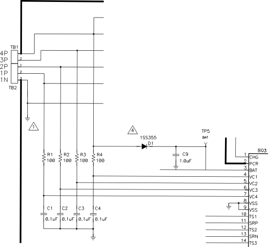 Figure 17. Cell and BAT Inputs
9.2.2.3.2 External Cell Balancing
Internal cell balancing can only support up to 10 mA. External cell balancing provides another option for faster cell balancing. For details, refer to the application note, Fast Cell Balancing Using External MOSFET (SLUA420).
9.2.2.3.3 PACK and FET Control
The PACK and VCC inputs provide power to the bq305x from the charger. The PACK input also provides a method to measure and detect the presence of a charger. The PACK input uses a 10-KΩ resistor, whereas the VCC input uses a diode to guard against input transients and prevents malfunction of the date driver during short-circuit events (Figure 18).
The N-channel charge and discharge FETs are controlled with 5.1-KΩ series gate resistors, which provide a switching time constant of a few microseconds. The 3.01-MΩ resistors ensure that the FETs are off in the event of an open connection to the FET drivers. Q4 is provided to protect the discharge FET (Q3) in the event of a reverse-connected charger. Without Q4, Q3 can be driven into its linear region and suffer severe damage if the PACK+ input becomes slightly negative.
Q4 turns on in that case to protect Q3 by shorting its gate to source. To use the simple ground gate circuit, the FET must have a low gate turn-on threshold. If it is desired to use a more standard device, such as the 2N7000 as the reference schematic, the gate should be biased up to 3.3 V with a high-value resistor. The bq3050 device has the capability to provide a current-limited charging path typically used for low battery voltage or low temperature charging. The pre-charge FET is integrated into the bq3050 device, allowing users to only connect an external pre-charge load resistor via the PCR pin through the PCHGIN input. The bq3050 device supports up to 100-mA of pre-charge current. When selecting the external load resistor, user should take into account the max charger voltage and the Rdson of the internal pre-charge FET.
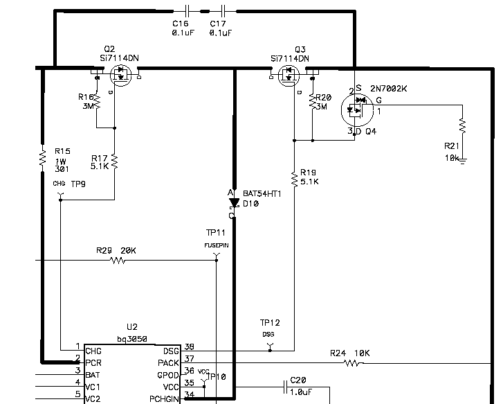 Figure 18. bq3050 PACK and FET Control
9.2.2.3.4 Regulator Output
As mentioned in Power Supply Decoupling and RBI, the two low-dropout regulators in the bq3050 require capacitive compensation on the output. The outputs must have a 1-μF ceramic capacitor placed close to the IC terminal pins.
9.2.2.3.5 Temperature Output
For the bq3050 device, TS1 and TS2 provide thermistor drive-under program control (Figure 19). Each pin can be enabled with an integrated 18-kΩ (typical) linearization pullup resistor to support the use of a 10-kΩ at 25°C (103) NTC external thermistor, such as a Mitsubishi BN35-3H103. The reference design includes two 10-kΩ thermistors: RT1 and RT2.
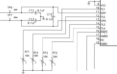 Figure 19. Thermistor Drive
9.2.2.3.6 LEDs
The LEDs do not need current-limiting resistors, because the bq3050 LED pins have a programmable current sink to simplify the design (Figure 20). The display switch pulls the bq3050 pin 20 to ground to generate an interrupt. The REG33 output powers the LEDs.
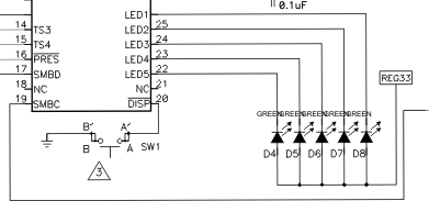 Figure 20. LEDs
9.2.2.3.7 Safety PTC Thermistor
The bq3050 device provides support for a safety PTC thermistor (Figure 21). The PTC thermistor is connected between the PTC pin and VSS. It can be placed close to the CHG/DSG FETs to monitor the temperature. The PTC pin outputs a very small current, typical approximate 370 nA, and the PTC fault will be triggered at approximately 0.7 V typical. A PTC fault is one of the permanent failure modes. It can only be cleared by a POR.
To disable this feature, connect a 10-KΩ resistor between PTC and VSS.
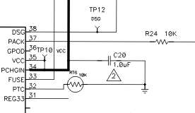 Figure 21. PTC Thermistor
9.2.2.4 Secondary-Overvoltage Protection
The bq29705 provides secondary-overvoltage protection and commands the chemical fuse to ignite if any cell exceeds the internally referenced threshold. The peripheral components are Cell Inputs and Time Delay Capacitor.
9.2.2.4.1 Cell Inputs
An input filter is provided for each cell input. This comprises the resistors R5, R6, R7, and R9 along with capacitors C5, C6, C7, and C8 (Figure 22). This input network is completely independent of the filter network used as input to thebq3050. To ensure independent safety functionality, the two devices must have separate input filters.
Because the filter capacitors are implemented differentially, a low-voltage device can be used in each case.
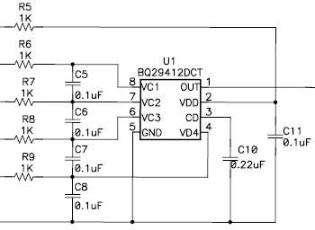 Figure 22. bq29705 Cell Inputs and Time-Delay Capacitor
9.2.2.4.2 Time-Delay Capacitor
C10 sets the time delay for activation of the output after any cell exceeds the threshold voltage. The time delay is calculated as td = 1.2 V × DelayCap (μF)/0.18 μA.
9.2.3 Application Curves
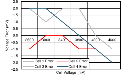 Figure 23. Cell Voltage Error Across Input Range at 25°C
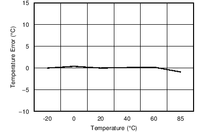 Figure 25. TSx Error vs. Temperature
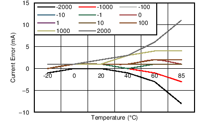 Figure 24. Current Error vs. Temperature
