SLUSA92D January 2011 – May 2015
PRODUCTION DATA.
- 1 Features
- 2 Applications
- 3 Description
- 4 Simplified Schematic
- 5 Revision History
- 6 Pin Configuration and Functions
-
7 Specifications
- 7.1 Absolute Maximum Ratings
- 7.2 ESD Ratings
- 7.3 Recommended Operating Conditions
- 7.4 Thermal Information
- 7.5 Supply Current
- 7.6 Power-On Reset (POR)
- 7.7 WAKE FROM SLEEP
- 7.8 RBI RAM Backup
- 7.9 3.3-V Regulator
- 7.10 2.5-V Regulator
- 7.11 DISP, PRES, SMBD, SMBC
- 7.12 CHG, DSG FET Drive
- 7.13 Internal Precharge Limiting
- 7.14 GPOD
- 7.15 FUSE
- 7.16 LED5, LED4, LED3, LED2, LED1
- 7.17 Coulomb Counter
- 7.18 VC1, VC2, VC3, VC4
- 7.19 TS1, TS2
- 7.20 Internal Temperature Sensor
- 7.21 Internal Thermal Shutdown
- 7.22 High Frequency Oscillator
- 7.23 Low Frequency Oscillator
- 7.24 Internal Voltage Reference
- 7.25 Flash
- 7.26 OCD Current Protection
- 7.27 SCD1 Current Protection
- 7.28 SCD2 Current Protection
- 7.29 SCC Current Protection
- 7.30 SBS Timing Requirements
- 7.31 Typical Characteristics
- 8 Detailed Description
- 9 Application and Implementation
- 10Power Supply Recommendations
- 11Layout
- 12Device and Documentation Support
- 13Mechanical, Packaging, and Orderable Information
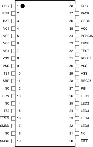
6 Pin Configuration and Functions
Pin Functions
| PIN NAME | PIN NUMBER | TYPE(1) | DESCRIPTION |
|---|---|---|---|
| CHG | 1 | O | Charge N-FET gate drive |
| PCR | 2 | O | Internal Precharge FET output |
| BAT | 3 | P | Alternate power source |
| VC1 | 4 | I | Sense input for positive voltage of top most cell in stack and cell balancing input for top most cell in stack |
| VC2 | 5 | I | Sense input for positive voltage of third lowest cell in stack and cell balancing input for third lowest cell in stack |
| VC3 | 6 | I | Sense input for positive voltage of second lowest cell in stack and cell balancing input for second lowest cell in stack |
| VC4 | 7 | I | Sense input for positive voltage of lowest cell in stack and cell balancing input for lowest cell in stack |
| VSS | 8 | P | Device ground |
| VSS | 9 | P | Device ground |
| TS1 | 10 | AI | Temperature sensor 1 thermistor input |
| SRP | 11 | AI | Differential Coulomb Counter input |
| NC | 12 | — | Not internally connected. Connect to VSS. |
| SRN | 13 | AI | Differential Coulomb Counter input |
| NC | 14 | — | Not internally connected. Connect to VSS. |
| TS2 | 15 | AI | Temperature sensor 2 thermistor input |
| PRES | 16 | I | Host system present input |
| SMBD | 17 | I/OD | SMBus v1.1 data line |
| NC | 18 | — | Not internally connected. Connect to VSS. |
| SMBC | 19 | I/OD | SMBus v1.1 clock line |
| DISP | 20 | I | Display active input |
| NC | 21 | — | Not internally connected. Connect to VSS. |
| LED5 | 22 | O | LED display constant current sink |
| LED4 | 23 | O | LED display constant current sink |
| LED3 | 24 | O | LED display constant current sink |
| LED2 | 25 | O | LED display constant current sink |
| LED1 | 26 | O | LED display constant current sink |
| RBI | 27 | P | RAM backup |
| REG25 | 28 | P | 2.5-V regulator output |
| VSS | 29 | P | Device ground |
| VSS | 30 | P | Device ground |
| REG33 | 31 | P | 3.3-V regulator output |
| TEST | 32 | — | Test pin, connect to VSS through 10-kΩ resistor |
| FUSE | 33 | O | Fuse drive |
| PCHGIN | 34 | I | Internal Precharge FET input |
| VCC | 35 | P | Power supply voltage |
| GPOD | 36 | I/OD | High voltage general purpose I/O |
| PACK | 37 | P | Alternate power source |
| DSG | 38 | O | Discharge N-FET gate drive |
(1) P = Power Connection, O = Digital Output, AI = Analog Input, I = Digital Input, I/OD = Digital Input/Output
