JAJSPG0 December 2022 BQ34Z100-R2
PRODUCTION DATA
- 1 特長
- 2 アプリケーション
- 3 概要
- 4 Revision History
- 5 Pin Configuration and Functions
-
6 Specifications
- 6.1 Absolute Maximum Ratings
- 6.2 ESD Ratings
- 6.3 Recommended Operating Conditions
- 6.4 Thermal Information
- 6.5 Electrical Characteristics: Power-On Reset
- 6.6 Electrical Characteristics: LDO Regulator
- 6.7 Electrical Characteristics: Internal Temperature Sensor Characteristics
- 6.8 Electrical Characteristics: Low-Frequency Oscillator
- 6.9 Electrical Characteristics: High-Frequency Oscillator
- 6.10 Electrical Characteristics: Integrating ADC (Coulomb Counter) Characteristics
- 6.11 Electrical Characteristics: ADC (Temperature and Cell Measurement) Characteristics
- 6.12 Electrical Characteristics: Data Flash Memory Characteristics
- 6.13 Timing Requirements: HDQ Communication
- 6.14 Timing Requirements: I2C-Compatible Interface
- 6.15 Typical Characteristics
- 7 Functional Block Diagram
-
8 Application and Implementation
- 8.1 Application Information
- 8.2
Typical Applications
- 8.2.1 Design Requirements
- 8.2.2
Detailed Design Procedure
- 8.2.2.1
Step-by-Step Design Procedure
- 8.2.2.1.1 STEP 1: Review and Modify the Data Flash Configuration Data.
- 8.2.2.1.2 STEP 2: Review and Modify the Data Flash Configuration Registers.
- 8.2.2.1.3 STEP 3: Design and Configure the Voltage Divider.
- 8.2.2.1.4 STEP 4: Determine the Sense Resistor Value.
- 8.2.2.1.5 STEP 5: Review and Modify the Data Flash Gas Gauging Configuration, Data, and State.
- 8.2.2.1.6 STEP 6: Determine and Program the Chemical ID.
- 8.2.2.1.7 STEP 7: Calibrate.
- 8.2.2.1.8 STEP 8: Run an Optimization Cycle.
- 8.2.2.1
Step-by-Step Design Procedure
- 9 Power Supply Recommendations
- 10Layout
- 11Device and Documentation Support
- 12Mechanical, Packaging, and Orderable Information
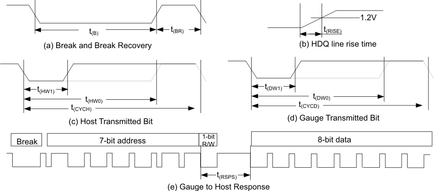
6.13 Timing Requirements: HDQ Communication
TA = –40°C to 85°C, 2.45 V < VREGIN = VBAT < 5.5 V; typical values at TA = 25°C and VREGIN = VBAT = 3.6 V (unless otherwise noted)
| PARAMETER | TEST CONDITIONS | MIN | NOM | MAX | UNIT | |
|---|---|---|---|---|---|---|
| t(CYCH) | Cycle time, host to BQ34Z100-R2 | 190 | μs | |||
| t(CYCD) | Cycle time, BQ34Z100-R2 to host | 190 | 205 | 250 | μs | |
| t(HW1) | Host sends 1 to BQ34Z100-R2 | 0.5 | 50 | μs | ||
| t(DW1) | BQ34Z100-R2 sends 1 to host | 32 | 50 | μs | ||
| t(HW0) | Host sends 0 to BQ34Z100-R2 | 86 | 145 | μs | ||
| t(DW0) | BQ34Z100-R2 sends 0 to host | 80 | 145 | μs | ||
| t(RSPS) | Response time, BQ34Z100-R2 to host | 190 | 950 | μs | ||
| t(B) | Break time | 190 | μs | |||
| t(BR) | Break recovery time | 40 | μs | |||
| t(RISE) | HDQ line rising time to logic 1 (1.2 V) | 950 | ns | |||
| t(RST) | HDQ Reset | 1.8 | 2.2 | s | ||
 Figure 6-1 Timing Diagrams