JAJSH51C August 2000 – March 2024 BUF634
PRODUCTION DATA
- 1
- 1 特長
- 2 アプリケーション
- 3 概要
- 4 Device Comparison Table
- 5 Pin Configuration and Functions
-
6 Specifications
- 6.1 Absolute Maximum Ratings
- 6.2 ESD Ratings
- 6.3 Recommended Operating Conditions
- 6.4 Thermal Information
- 6.5 Electrical Characteristics: TO-220 and TO-263 Packages
- 6.6 Electrical Characteristics: Wide-Bandwidth Mode for SOIC Package
- 6.7 Electrical Characteristics: Low-Quiescent-Current Mode for SOIC Package
- 6.8 Typical Characteristics: TO-220 and TO-263 Packages
- 6.9 Typical Characteristics: SOIC Package
- 7 Detailed Description
- 8 Application and Implementation
- 9 Device and Documentation Support
- 10Revision History
- 11Mechanical, Packaging, and Orderable Information
パッケージ・オプション
メカニカル・データ(パッケージ|ピン)
サーマルパッド・メカニカル・データ
- KTT|5
発注情報
8.1.1 High Frequency Applications
The excellent bandwidth and fast slew rate of the BUF634 device are useful in a variety of high frequency open-loop applications. When operated open-loop, printed-circuit-board layout and bypassing technique can affect dynamic performance.
For best results, use a ground plane-type circuit board layout and bypass the power supplies with 0.1-µF ceramic chip capacitors at the device pins in parallel with solid tantalum 10-µF capacitors. Source resistance affects high-frequency peaking, step-response overshoot and ringing. Best response is usually achieved with a series input resistor of 25 Ω to 200 Ω, depending on the signal source. Response with some loads (especially capacitive) can be improved with a resistor of 10 Ω to 150 Ω in series with the output.
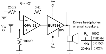
 Figure 8-2 High Performance Headphone Driver
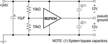
 Figure 8-3 Pseudo-Ground Driver
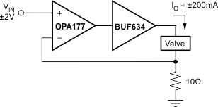
 Figure 8-4 Current-Output Valve Driver
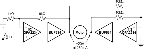
 Figure 8-5 Bridge-Connected Motor Driver