SCAS862G November 2008 – July 2016 CDCE62005
PRODUCTION DATA.
- 1 Features
- 2 Applications
- 3 Description
- 4 Revision History
- 5 Pin Configuration and Functions
- 6 Specifications
- 7 Parameter Measurement Information
-
8 Detailed Description
- 8.1 Overview
- 8.2 Functional Block Diagrams
- 8.3
Feature Description
- 8.3.1 Phase Noise Analysis
- 8.3.2 Output To Output Isolation
- 8.3.3 Device Control
- 8.3.4 External Control Pins
- 8.3.5
Input Block
- 8.3.5.1 Universal Input Buffers (UIB)
- 8.3.5.2 LVDS Fail Safe Mode
- 8.3.5.3 Smart Multiplexer Controls
- 8.3.5.4 Smart Multiplexer Auto Mode
- 8.3.5.5 Smart Multiplexer Dividers
- 8.3.5.6 Output Block
- 8.3.5.7 Output Multiplexer Control
- 8.3.5.8 Output Buffer Control
- 8.3.5.9 Output Buffer Control - LVCMOS Configurations
- 8.3.5.10 Output Dividers
- 8.3.5.11 Digital Phase Adjust
- 8.3.5.12 Phase Adjust Example
- 8.3.5.13 Valid Register Settings for Digital Phase Adjust Blocks
- 8.3.5.14 Output Synchronization
- 8.3.5.15 Auxiliary Output
- 8.3.5.16 Synthesizer Block
- 8.3.5.17 Input Divider
- 8.3.5.18 Feedback and Feedback Bypass Divider
- 8.3.5.19 Internal Loop Filter Component Configuration
- 8.3.5.20 External Loop Filter Component Configuration
- 8.3.6 Digital Lock Detect
- 8.3.7 Crystal Input Interference
- 8.3.8 VCO Calibration
- 8.3.9 Startup Time Estimation
- 8.3.10 Analog Lock Detect
- 8.4 Device Functional Modes
- 8.5 Programming
- 8.6
Register Maps
- 8.6.1 Device Registers: Register 0 Address 0x00
- 8.6.2 Device Registers: Register 1 Address 0x01
- 8.6.3 Device Registers: Register 2 Address 0x02
- 8.6.4 Device Registers: Register 3 Address 0x03
- 8.6.5 Device Registers: Register 4 Address 0x04
- 8.6.6 Device Registers: Register 5 Address 0x05
- 8.6.7 Device Registers: Register 6 Address 0x06
- 8.6.8 Device Registers: Register 7 Address 0x07
- 8.6.9 Device Registers: Register 8 Address 0x08
- 9 Application and Implementation
- 10Power Supply Recommendations
- 11Layout
- 12Device and Documentation Support
- 13Mechanical, Packaging, and Orderable Information
パッケージ・オプション
メカニカル・データ(パッケージ|ピン)
- RGZ|48
サーマルパッド・メカニカル・データ
- RGZ|48
発注情報
9 Application and Implementation
NOTE
Information in the following applications sections is not part of the TI component specification, and TI does not warrant its accuracy or completeness. TI’s customers are responsible for determining suitability of components for their purposes. Customers should validate and test their design implementation to confirm system functionality.
9.1 Application Information
9.1.1 Frequency Synthesizer
As shown in Figure 47, the CDCE62005 has internal dividers, twin onboard VCOs, a phase frequency detector, charge pump, partially internal loop filter, and LVPECL/LVDS/LVCMOS input and output buffers, all of which completes a PLL. Through the PLL operation, the VCO clock synchronizes with the reference clock input and ultimately with all clock outputs. All outputs are completely synchronized in terms of phase and frequency with the reference clock input. When powering up from the EEPROM, the SYNC signal synchronizes outputs after device power-up.
See SCAA096 for a detailed description of the application configuration.
9.2 Typical Application
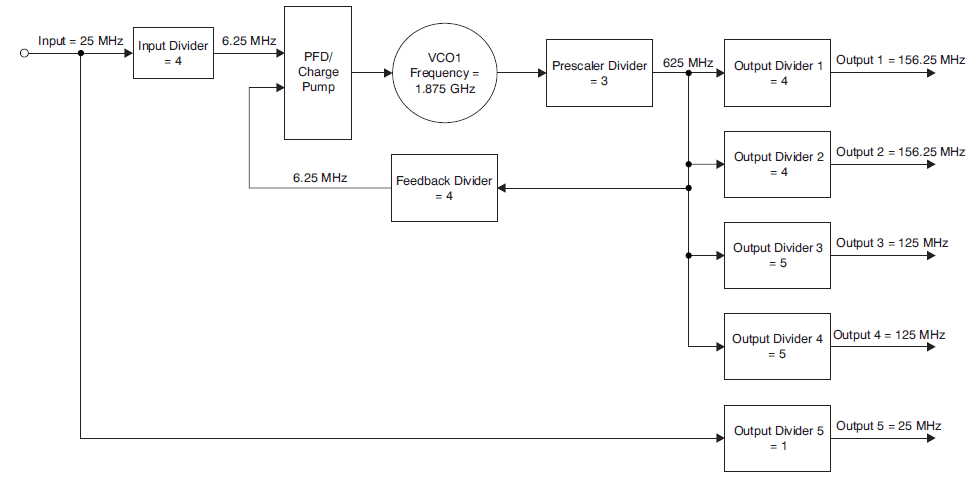 Figure 47. CDCE62005 Settings for Multiple Frequency Synthesis Example
9.2.1 Design Requirements
Assume a typical application, where a total of two 156.25-MHz LVPECL, two 125-MHz LVDS, and two 25-MHz LVCMOS output clocks are desired and should be phase-locked to a single back-plane input reference clock of 25 MHz. The goal of this example is to identify the input (M), prescaler (N), feedback (FB), and output (P) divider values, the VCO frequency to lock to, and the other related PLL settings needed to derive the different output frequencies from the common input and VCXO frequencies. Follow the steps outlined in Detailed Design Procedure to achieve this goal.
9.2.2 Detailed Design Procedure
Step 1. From Figure 47, it can be inferred that the relationship between the output frequency and the input frequency is described by these equations,
where:
provided that:
and:
Step 2. Keep in mind the following while satisfying the equations in Step 1:
- The P divider can be chosen to be 1, 2, 3, 4, 5, up to 80
- The internal VCO range is from 1.75 GHz to 2.35 GHz
- The input (M) and prescaler (N) dividers can be chosen from Table 22 and Table 26.
- The FB divider can be chosen from the values in Table 23 and Table 24.
Step 3. Given multiple desired output frequencies and the input frequency, the first step would be to establish M, N, and FB divider values for different P divider settings to satisfy these equations:
Such that these parameters are valid:
- The common PFD frequency is always less than 40 MHz.
- The VCXO frequency is the same for deriving all outputs.
Using the example to derive these outputs, it can be seen that there is not an output divider (P5) that will generate a 25-MHz output. However, the output MUX value of output 5 can be chosen to directly bypass the 25-MHz input clock to output 5. Therefore, in order to use a common VCO frequency, the P dividers to be used are:
- P1 = 4
- P2 = 4
- P3 = 5
- P4 = 5
- P5 = 1
The common VCO frequency is 1875 MHz and is VCO1. The output MUX for outputs 1 to 4 are set to the PLL/VCO outputs. Moreover, the FB divider to be used is:
The N divider to be used is:
These values ensure that the (FIN/M) ratio is within 40 MHz and is set at 6.25 MHz. Thus, the M divider to be used is:
Figure 47 illustrates this configuration.
Step 4:
The PLL loop bandwidth of the CDCE62005 is recommended to be set according to the phase noise profile of its reference input and the phase noise profile of the onboard VCO clock. It is recommended to set the PLL loop bandwidth as the crossover point of the reference input phase noise and the phase noise of the VCO clock. When the input clock is clean and any near-frequency offsets are better than the VCO clock, it is beneficial for the PLL bandwidth to be set at several hundred kHz as determined by the crossover point. Figure 48 shows a typical 400-kHz Loop filter.
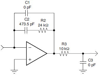 Figure 48. On-Chip Loop Filter Circuit for 400-kHz Loop Bandwidth
(Loop Settings in Figure 47, CP Current at 3.5mA)
9.2.3 Application Curves
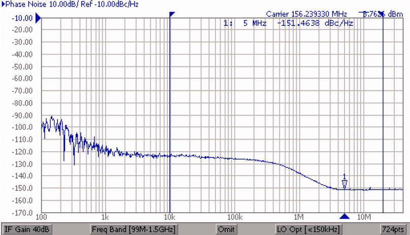
RMS Jitter is 520 fsec (10 kHz to 20 MHz)
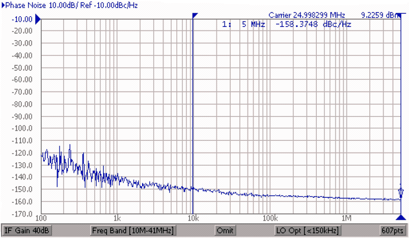
RMS Jitter is 261 fsec (10 kHz to 5 MHz)
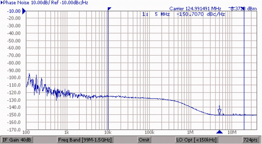
RMS Jitter is 540 fsec (10 kHz to 20 MHz)