JAJSED0G May 2012 – January 2018 CDCM6208
PRODUCTION DATA.
- 1 特長
- 2 アプリケーション
- 3 概要
- 4 改訂履歴
- 5 Pin Configuration and Functions
-
6 Specifications
- 6.1 Absolute Maximum Ratings
- 6.2 ESD Ratings
- 6.3 Recommended Operating Conditions
- 6.4 Thermal Information, Airflow = 0 LFM
- 6.5 Thermal Information, Airflow = 150 LFM
- 6.6 Thermal Information, Airflow = 250 LFM
- 6.7 Thermal Information, Airflow = 500 LFM
- 6.8 Single-Ended Input Characteristics (SI_MODE[1:0], SDI/SDA/PIN1, SCL/PIN4, SDO/ADD0/PIN2, SCS/ADD1/PIN3, STATUS1/PIN0, RESETN/PWR, PDN, SYNCN, REF_SEL)
- 6.9 Single-Ended Input Characteristics (PRI_REF, SEC_REF)
- 6.10 Differential Input Characteristics (PRI_REF, SEC_REF)
- 6.11 Crystal Input Characteristics (SEC_REF)
- 6.12 Single-Ended Output Characteristics (STATUS1, STATUS0, SDO, SDA)
- 6.13 PLL Characteristics
- 6.14 LVCMOS Output Characteristics
- 6.15 LVPECL (High-Swing CML) Output Characteristics
- 6.16 CML Output Characteristics
- 6.17 LVDS (Low-Power CML) Output Characteristics
- 6.18 HCSL Output Characteristics
- 6.19 Output Skew and Sync to Output Propagation Delay Characteristics
- 6.20 Device Individual Block Current Consumption
- 6.21 Worst Case Current Consumption
- 6.22 Timing Requirements, I2C Timing
- 6.23 Typical Characteristics
- 7 Parameter Measurement Information
-
8 Detailed Description
- 8.1 Overview
- 8.2 Functional Block Diagram
- 8.3
Feature Description
- 8.3.1 Typical Device Jitter
- 8.3.2 Universal Input Buffer (PRI_REF, SEC_REF)
- 8.3.3 VCO Calibration
- 8.3.4 Reference Divider (R)
- 8.3.5 Input Divider (M)
- 8.3.6 Feedback Divider (N)
- 8.3.7 Prescaler Dividers (PS_A, PS_B)
- 8.3.8 Phase Frequency Detector (PFD)
- 8.3.9 Charge Pump (CP)
- 8.3.10 Fractional Output Divider Jitter Performance
- 8.3.11 Device Block-Level Description
- 8.3.12 Device Configuration Control
- 8.3.13 Configuring the RESETN Pin
- 8.3.14 Preventing False Output Frequencies in SPI/I2C Mode at Start-Up
- 8.3.15 Input MUX and Smart Input MUX
- 8.4 Device Functional Modes
- 8.5 Programming
- 8.6 Register Maps
-
9 Application and Implementation
- 9.1 Application Information
- 9.2
Typical Applications
- 9.2.1 Design Requirements
- 9.2.2
Detailed Design Procedures
- 9.2.2.1 Jitter Considerations in SERDES Systems
- 9.2.2.2 Jitter Considerations in ADC and DAC Systems
- 9.2.2.3 Configuring the PLL
- 9.2.2.4 Programmable Loop Filter
- 9.2.2.5 Loop filter Component Selection
- 9.2.2.6 Device Output Signaling
- 9.2.2.7 Integer Output Divider (IO)
- 9.2.2.8 Fractional Output Divider (FOD)
- 9.2.2.9 Output Synchronization
- 9.2.2.10 Output Mux on Y4 and Y5
- 9.2.2.11 Staggered CLK Output Power Up for Power Sequencing of a DSP
- 10Power Supply Recommendations
- 11Layout
- 12デバイスおよびドキュメントのサポート
- 13メカニカル、パッケージ、および注文情報
パッケージ・オプション
メカニカル・データ(パッケージ|ピン)
- RGZ|48
サーマルパッド・メカニカル・データ
- RGZ|48
発注情報
9.2.2.2 Jitter Considerations in ADC and DAC Systems
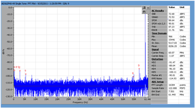
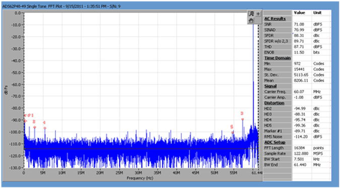
A/D and D/A converters are sensitive to clock jitter in two ways: They are sensitive to phase noise in a particular frequency band, and also have maximum spur level requirements to achieve maximum noise floor sensitivity. The following test results were achieved connecting the CDCM6208 to ADC and DACs:
 Figure 52. IF = 60 MHz Fclk = 122.88 MHz Baseline (Lab Clk Generator) ADC: ADS62P48-49
 Figure 53. IF = 60 MHz Fclk = 122.88 MHz CDCM6208 Driving ADC
Observation: Up to an IF = 100 MHz, the ADC performance when driven by the CDCM6208 (Figure 53) is similar to when the ADC is driven by an expensive lab signal generator with additional passive source filtering (Figure 52).
Conclusion: Therefore, the CDCM6208 is usable for applications up to 100 MHz IF. For IF above 100 MHz, the SNR starts degrading in our experiments. Measurements were conducted with ADC connected to Y0 and other outputs running at different integer frequencies.
NOTE
For crosstalk, TI highly recommends configuring both pre-dividers identically, otherwise the SFDR and SNR suffer due to crosstalk between the two pre-divider frequencies.
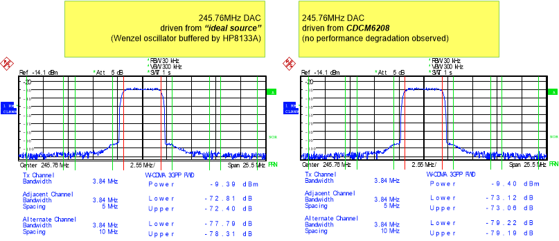
 Figure 54. DAC Driven by Lab Source and CDCM6208 in Comparison (Performance Identical)
Observation/Conclusion: The DAC performance was not degraded at all by the CDCM6208 compared to driving the DAC with a perfect lab source. Therefore, the CDCM6208 provides sufficient low noise to drive a 245.76 MHz DAC.