SLPS319C June 2012 – January 2015 CSD18501Q5A
PRODUCTION DATA.
- 1Features
- 2Applications
- 3Description
- 4Revision History
- 5Specifications
- 6Device and Documentation Support
- 7Mechanical, Packaging, and Orderable Information
パッケージ・オプション
デバイスごとのパッケージ図は、PDF版データシートをご参照ください。
メカニカル・データ(パッケージ|ピン)
- DQJ|8
サーマルパッド・メカニカル・データ
発注情報
5 Specifications
5.1 Electrical Characteristics
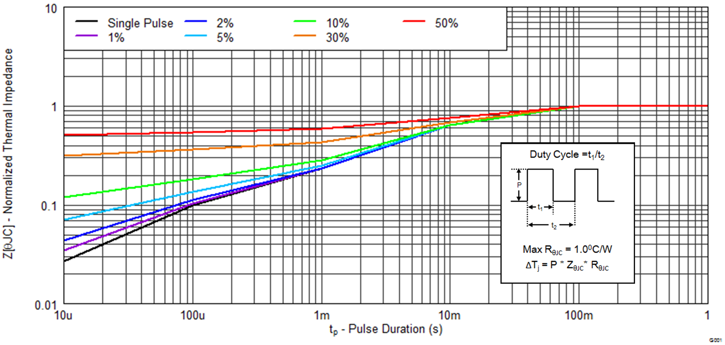
(TA = 25°C unless otherwise stated)5.2 Thermal Information
(TA = 25°C unless otherwise stated)| THERMAL METRIC | MIN | TYP | MAX | UNIT | |
|---|---|---|---|---|---|
| RθJC | Junction-to-Case Thermal Resistance(1) | 1.0 | °C/W | ||
| RθJA | Junction-to-Ambient Thermal Resistance(1)(2) | 50 | |||
(1) RθJC is determined with the device mounted on a 1-inch2 (6.45-cm2), 2-oz. (0.071-mm thick) Cu pad on a 1.5-inches × 1.5-inches
(3.81-cm × 3.81-cm), 0.06-inch (1.52-mm) thick FR4 PCB. RθJC is specified by design, whereas RθJA is determined by the user’s board design.
(3.81-cm × 3.81-cm), 0.06-inch (1.52-mm) thick FR4 PCB. RθJC is specified by design, whereas RθJA is determined by the user’s board design.
(2) Device mounted on FR4 material with 1-inch2 (6.45-cm2), 2-oz. (0.071-mm thick) Cu.
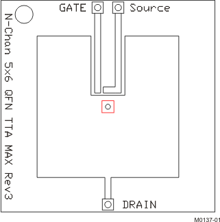 |
Max RθJA = 50°C/W when mounted on 1 inch2 (6.45-cm2) of 2-oz. (0.071-mm thick) Cu. |
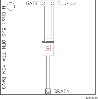 |
Max RθJA = 125°C/W when mounted on a minimum pad area of 2-oz. (0.071-mm thick) Cu. |
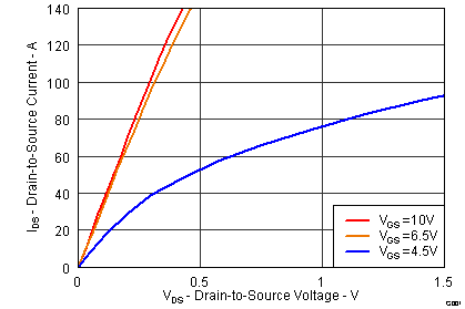
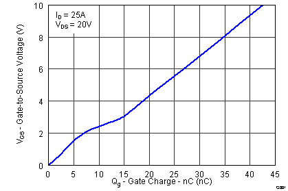
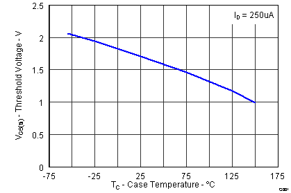
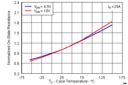
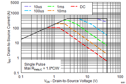
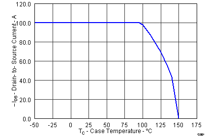
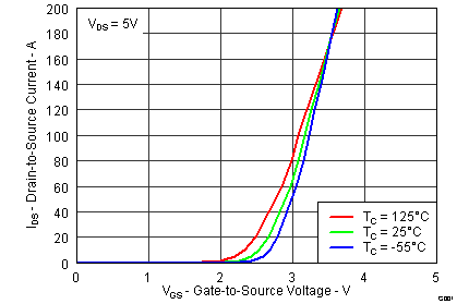
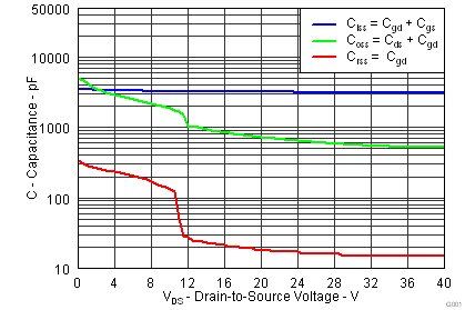
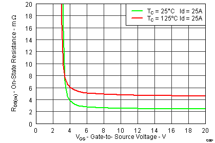
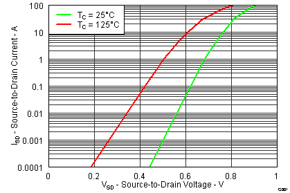
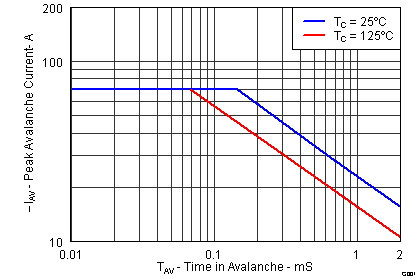
5.3 Typical MOSFET Characteristics
(TA = 25°C unless otherwise stated)