JAJSAQ5F December 2007 – October 2016 DAC121C081 , DAC121C085
PRODUCTION DATA.
- 1 特長
- 2 アプリケーション
- 3 概要
- 4 改訂履歴
- 5 概要(続き)
- 6 Pin Configuration and Functions
- 7 Specifications
- 8 Detailed Description
- 9 Application and Implementation
- 10Power Supply Recommendations
- 11Layout
- 12デバイスおよびドキュメントのサポート
- 13メカニカル、パッケージ、および注文情報
パッケージ・オプション
メカニカル・データ(パッケージ|ピン)
サーマルパッド・メカニカル・データ
発注情報
7 Specifications
7.1 Absolute Maximum Ratings
over operating free-air temperature range (unless otherwise noted)(1)(2)(3)| MIN | MAX | UNIT | |||
|---|---|---|---|---|---|
| Supply voltage, VA | –0.3 | 6.5 | V | ||
| Voltage on any input pin | –0.3 | 6.5 | V | ||
| Input current at any pin(4) | ±10 | mA | |||
| Package input current(4) | ±20 | mA | |||
| Power consumption at TA = 25°C | See(5) | ||||
| Junction temperature, TJ | 150 | °C | |||
| Storage temperature, Tstg | –65 | 150 | °C | ||
(1) Stresses beyond those listed under Absolute Maximum Ratings may cause permanent damage to the device. These are stress ratings only, which do not imply functional operation of the device at these or any other conditions beyond those indicated under Recommended Operating Conditions. Exposure to absolute-maximum-rated conditions for extended periods may affect device reliability.
(2) All voltages are measured with respect to GND = 0 V, unless otherwise specified.
(3) If Military/Aerospace specified devices are required, contact the Texas Instruments Sales Office/ Distributors for availability and specifications.
(4) When the input voltage at any pin exceeds 5.5 V or is less than GND, the current at that pin should be limited to 10 mA. The 20-mA maximum package input current ratings limits the number of pins that can safely exceed the power supplies with an input current of 10 mA to two.
(5) The absolute maximum junction temperature (TJmax) for this device is 150°C. The maximum allowable power dissipation is dictated by TJmax, the junction-to-ambient thermal resistance (θJA), and the ambient temperature (TA), and can be calculated using the formula PDMAX = (TJmax − TA) / θJA. The values for maximum power dissipation will be reached only when the device is operated in a severe fault condition (for example, when input or output pins are driven beyond the operating ratings, or the power supply polarity is reversed).
7.2 ESD Ratings
| VALUE | UNIT | ||||
|---|---|---|---|---|---|
| DAC081C081 in NGF Package | |||||
| V(ESD) | Electrostatic discharge | Human-body model (HBM), per ANSI/ESDA/JEDEC JS-001 | All pins except 2 and 3 | ±2500 | V |
| Pins 2 and 3 | ±5000 | ||||
| Charged-device model (CDM), per JEDEC specification JESD22-C101 | All pins except 2 and 3 | ±1000 | |||
| Pins 2 and 3 | ±1000 | ||||
| Machine model (MM) | All pins except 2 and 3 | ±250 | |||
| Pins 2 and 3 | ±350 | ||||
| DAC081C081 in DDC Package | |||||
| V(ESD) | Electrostatic discharge | Human-body model (HBM), per ANSI/ESDA/JEDEC JS-001 | All pins except 4 and 5 | ±2500 | V |
| Pins 4 and 5 | ±5000 | ||||
| Charged-device model (CDM), per JEDEC specification JESD22-C101 | All pins except 4 and 5 | ±1000 | |||
| Pins 4 and 5 | ±1000 | ||||
| Machine model (MM) | All pins except 4 and 5 | ±250 | |||
| Pins 4 and 5 | ±350 | ||||
| DAC081C085 in DGK Package | |||||
| V(ESD) | Electrostatic discharge | Human-body model (HBM), per ANSI/ESDA/JEDEC JS-001 | All pins except 3 and 4 | ±2500 | V |
| Pins 3 and 4 | ±5000 | ||||
| Charged-device model (CDM), per JEDEC specification JESD22-C101 | All pins except 3 and 4 | ±1000 | |||
| Pins 3 and 4 | ±1000 | ||||
| Machine model (MM) | All pins except 3 and 4 | ±250 | |||
| Pins 3 and 4 | ±350 | ||||
7.3 Recommended Operating Conditions
over operating free-air temperature range (unless otherwise noted)(1)| MIN | MAX | UNIT | |
|---|---|---|---|
| Operating temperature, TA | −40 | 125 | °C |
| Supply voltage, VA | 2.7 | 5.5 | V |
| Reference voltage, VREFIN | 1 | VA | V |
| Digital input voltage(2) | 0 | 5.5 | V |
| Output load | 0 | 1500 | pF |
(1) All voltages are measured with respect to GND = 0 V, unless otherwise specified.
(2) The inputs are protected as shown in the following. Input voltage magnitudes up to 5.5 V, regardless of VA, will not cause errors in the conversion result. For example, if VA is 3 V, the digital input pins can be driven with a 5-V logic device.
7.4 Thermal Information
| THERMAL METRIC(1)(2)(3) | DAC121C081 | DAC121C085 | UNIT | ||
|---|---|---|---|---|---|
| NGF (WSON) | DDC (SOT) | DGK (VSSOP) | |||
| 6 PINS | 6 PINS | 8 PINS | |||
| RθJA | Junction-to-ambient thermal resistance | 190 | 250 | 240 | °C/W |
(1) For more information about traditional and new thermal metrics, see the Semiconductor and IC Package Thermal Metrics application report.
(2) Soldering process must comply with Texas Instruments' Reflow Temperature Profile Specifications, SNOA549.
(3) Reflow temperature profiles are different for lead-free packages.
7.5 Electrical Characteristics
The following specifications apply for VA = 2.7 V to 5.5 V, VREF = VA, CL = 200 pF to GND, input code range 48 to 4047. All Maximum and Minimum limits apply for TMIN ≤ TA ≤ TMAX and all Typical limits are at TA = 25°C, unless otherwise specified.(1)| PARAMETER | TEST CONDITIONS | MIN | TYP(3) | MAX(3) | UNIT | ||
|---|---|---|---|---|---|---|---|
| STATIC PERFORMANCE | |||||||
| INL | Resolution | 12 | Bits | ||||
| Monotonicity | 12 | Bits | |||||
| Integral Non-Linearity | 2.2 | 8 | LSB | ||||
| –8 | –1.5 | ||||||
| DNL | Differential Non-Linearity | 0.18 | 0.6 | LSB | |||
| –0.5 | –0.12 | LSB | |||||
| ZE | Zero Code Error | IOUT = 0 | 1.1 | 10 | mV | ||
| FSE | Full-Scale Error | IOUT = 0 | –0.1 | −0.7 | %FSR | ||
| GE | Gain Error | All ones Loaded to DAC register | –0.2 | −0.7 | %FSR | ||
| ZCED | Zero Code Error Drift | –20 | µV/°C | ||||
| TC GE | Gain Error Tempco | VA = 3 V | –0.7 | ppm FSR/°C | |||
| VA = 5 V | –1 | ||||||
| ANALOG OUTPUT CHARACTERISTICS (VOUT) | |||||||
| Output voltage range(4) | DAC121C085 | 0 | VREF | V | |||
| DAC121C081 | 0 | VA | |||||
| ZCO | Zero code output | VA = 3 V, IOUT = 200 µA | 1.3 | mV | |||
| VA = 5 V, IOUT = 200 µA | 7 | ||||||
| FSO | Full scale output | VA = 3 V, IOUT = 200 µA | 2.984 | V | |||
| VA = 5 V, IOUT = 200 µA | 4.989 | ||||||
| IOS | Output short-circuit current (ISOURCE) |
VA = 3 V, VOUT = 0 V, Input Code = FFFh. |
56 | mA | |||
| VA = 5 V, VOUT = 0 V, Input Code = FFFh. |
69 | ||||||
| IOS | Output short-circuit current (ISINK) |
VA = 3 V, VOUT = 3 V, Input Code = 000h. |
–52 | mA | |||
| VA = 5 V, VOUT = 5 V, Input Code = 000h. |
–75 | ||||||
| IO | Continuous output current(4) | Available on the DAC output | 11 | mA | |||
| CL | Maximum load capacitance | RL = ∞ | 1500 | pF | |||
| RL = 2 kΩ | 1500 | ||||||
| ZOUT | DC output impedance | 7.5 | Ω | ||||
| REFERENCE INPUT CHARACTERISTICS (DAC121C085 only) | |||||||
| VREF | Input range minimum | 1 | 0.2 | V | |||
| Input range maximum | VA | V | |||||
| Input impedance | 120 | kΩ | |||||
| LOGIC INPUT CHARACTERISTICS (SCL, SDA) | |||||||
| VIH | Input high voltage | 0.7 × VA | V | ||||
| VIL | Input low voltage | 0.3 × VA | V | ||||
| IIN | Input current | ±1 | µA | ||||
| CIN | Input pin capacitance(4) | 3 | pF | ||||
| VHYST | Input hysteresis | 0.1 × VA | V | ||||
| LOGIC INPUT CHARACTERISTICS (ADR0, ADR1) | |||||||
| VIH | Input high voltage | VA- 0.5 | V | ||||
| VIL | Input low voltage | 0.5 | V | ||||
| IIN | Input current | ±1 | µA | ||||
| LOGIC OUTPUT CHARACTERISTICS (SDA) | |||||||
| VOL | Output low voltage | ISINK = 3 mA | 0.4 | V | |||
| ISINK = 6 mA | 0.6 | ||||||
| IOZ | High-impedence output leakage current | ±1 | µA | ||||
| POWER REQUIREMENTS | |||||||
| VA | Supply voltage minimum | 2.7 | V | ||||
| Supply voltage maximum | 5.5 | ||||||
| Normal -- VOUT set to midscale. 2-wire interface quiet (SCL = SDA = VA). (output unloaded) | |||||||
| IST_VA-1 | VADAC121C081 supply current | VA = 2.7 V to 3.6 V | 105 | 156 | µA | ||
| VA = 4.5 V to 5.5 V | 132 | 214 | |||||
| IST_VA-5 | VADAC121C085 supply current | VA = 2.7 V to 3.6 V | 86 | 118 | µA | ||
| VA = 4.5 V to 5.5 V | 98 | 152 | |||||
| IST_VREF | VREF supply current (DAC121C085 only) |
VA = 2.7 V to 3.6 V | 37 | 43 | µA | ||
| VA = 4.5 V to 5.5 V | 53 | 61 | |||||
| PST | Power consumption (VA and VREF for DAC121C085)(2) |
VA = 3 V | 380 | µW | |||
| VA = 5 V | 730 | ||||||
| Continuous Operation -- 2-wire interface actively addressing the DAC and writing to the DAC register. (output unloaded) | |||||||
| ICO_VA-1 | VADAC121C081 supply current | fSCL=400 kHz | VA = 2.7 V to 3.6 V | 134 | 220 | µA | |
| VA = 4.5 V to 5.5 V | 192 | 300 | |||||
| fSCL = 3.4 MHz | VA = 2.7 V to 3.6 V | 225 | 320 | µA | |||
| VA = 4.5 V to 5.5 V | 374 | 500 | |||||
| ICO_VA-5 | VADAC121C085 supply current | fSCL = 400 kHz | VA = 2.7 V to 3.6 V | 101 | 155 | µA | |
| VA = 4.5 V to 5.5 V | 142 | 220 | |||||
| fSCL = 3.4 MHz | VA = 2.7 V to 3.6 V | 193 | 235 | µA | |||
| VA = 4.5 V to 5.5 V | 325 | 410 | |||||
| ICO_VREF | VREF supply current (DAC121C085 only) |
VA = 2.7 V to 3.6 V | 33.5 | 55 | µA | ||
| VA = 4.5 V to 5.5 V | 49.5 | 71.4 | |||||
| PCO | Power consumption (VA and VREF for DAC121C085) |
fSCL = 400 kHz | VA = 3 V | 480 | µW | ||
| VA = 5 V | 1.06 | mW | |||||
| fSCL = 3.4 MHz | VA = 3 V | 810 | µW | ||||
| VA = 5 V | 2.06 | mW | |||||
| Power Down -- 2-wire interface quiet (SCL = SDA = VA) after PD mode written to DAC register. (output unloaded) | |||||||
| IPD | Supply current (VA and VREF for DAC121C085) |
All power-down modes | VA = 2.7 V to 3.6 | 0.13 | 1.52 | µA | |
| VA = 4.5 V to 5.5 V | 0.15 | 3.25 | |||||
| PPD | Power consumption (VA and VREF for DAC121C085) |
All power-down modes | VA = 3 V | 0.5 | µW | ||
| VA = 5 V | 0.9 | ||||||
(1) Values shown in this table are design targets and are subject to change before product release.
7.6 AC and Timing Characteristics
The following specifications apply for VA = 2.7 V to 5.5 V, VREF = VA, RL = Infinity, CL = 200 pF to GND. All Maximum and Minimum limits apply for TMIN ≤ TA ≤ TMAX and all Typical limits are at TA = 25°C, unless otherwise specified.(1)| PARAMETER | TEST CONDITIONS(7) | MIN | TYP(3) | MAX(7)(3) | UNIT | ||
|---|---|---|---|---|---|---|---|
| ts | Output Voltage Settling Time(4) | 400h to C00h code change RL = 2 kΩ, CL = 200 pF |
6 | 8.5 | µs | ||
| SR | Output Slew Rate | 1 | V/µs | ||||
| Glitch Impulse | Code change from 800h to 7FFh | 12 | nV-sec | ||||
| Digital Feedthrough | 0.5 | nV-sec | |||||
| Multiplying Bandwidth(6) | VREF = 2.5 V ± 0.1 Vpp | 160 | kHz | ||||
| Total Harmonic Distortion(6) | VREF = 2.5 V ± 0.1 Vpp input frequency = 10 kHz |
70 | dB | ||||
| tWU | Wake-Up Time | VA = 3 V | 0.8 | µs | |||
| VA = 5 V | 0.5 | µs | |||||
| DIGITAL TIMING SPECS (SCL, SDA) | |||||||
| fSCL | Serial Clock Frequency | Standard Mode | 100 | kHz | |||
| Fast Mode | 400 | ||||||
| High Speed Mode, Cb = 100 pF | 3.4 | MHz | |||||
| High Speed Mode, Cb = 400 pF | 1.7 | ||||||
| tLOW | SCL Low Time | Standard Mode | 4.7 | µs | |||
| Fast Mode | 1.3 | ||||||
| High Speed Mode, Cb = 100 pF | 160 | ns | |||||
| High Speed Mode, Cb = 400 pF | 320 | ||||||
| tHIGH | SCL High Time | Standard Mode | 4 | µs | |||
| Fast Mode | 0.6 | ||||||
| High Speed Mode, Cb = 100 pF | 60 | ns | |||||
| High Speed Mode, Cb = 400 pF | 120 | ||||||
| tSU;DAT | Data Setup Time | Standard Mode | 250 | ns | |||
| Fast Mode | 100 | ||||||
| High Speed Mode | 10 | ||||||
| tHD;DAT | Data Hold Time | Standard Mode | 0 | 3.45 | µs | ||
| Fast Mode | 0 | 0.9 | |||||
| High Speed Mode, Cb = 100 pF | 0 | 70 | ns | ||||
| High Speed Mode, Cb = 400 pF | 0 | 150 | |||||
| tSU;STA | Setup time for a start or a repeated start condition | Standard Mode | 4.7 | µs | |||
| Fast Mode | 0.6 | ||||||
| High Speed Mode | 160 | ns | |||||
| tHD;STA | Hold time for a start or a repeated start condition | Standard Mode | 4 | µs | |||
| Fast Mode | 0.6 | ||||||
| High Speed Mode | 160 | ns | |||||
| tBUF | Bus free time between a stop and start condition | Standard Mode | 4.7 | µs | |||
| Fast Mode | 1.3 | ||||||
| tSU;STO | Setup time for a stop condition | Standard Mode | 4 | µs | |||
| Fast Mode | 0.6 | ||||||
| High Speed Mode | 160 | ns | |||||
| trDA | Rise time of SDA signal | Standard Mode | 1000 | ns | |||
| Fast Mode | 20+0.1Cb | 300 | |||||
| High Speed Mode, Cb = 100 pF | 10 | 80 | |||||
| High Speed Mode, Cb = 400 pF | 20 | 160 | |||||
| tfDA | Fall time of SDA signal | Standard Mode | 250 | ns | |||
| Fast Mode | 20+0.1Cb | 250 | |||||
| High Speed Mode, Cb = 100 pF | 10 | 80 | |||||
| High Speed Mode, Cb = 400 pF | 20 | 160 | |||||
| trCL | Rise time of SCL signal | Standard Mode | 1000 | ns | |||
| Fast Mode | 20+0.1Cb | 300 | |||||
| High Speed Mode, Cb = 100 pF | 10 | 40 | |||||
| High Speed Mode, Cb = 400 pF | 20 | 80 | |||||
| trCL1 | Rise time of SCL signal after a repeated start condition and after an acknowledge bit. | Standard Mode | 1000 | ns | |||
| Fast Mode | 20+0.1Cb | 300 | |||||
| High Speed Mode, Cb = 100 pF | 10 | 80 | |||||
| High Speed Mode, Cb = 400 pF | 20 | 160 | |||||
| tfCL | Fall time of a SCL signal | Standard Mode | 300 | ns | |||
| Fast Mode | 20+0.1Cb | 300 | |||||
| High Speed Mode, Cb = 100 pF | 10 | 40 | |||||
| High Speed Mode, Cb = 400 pF | 20 | 80 | |||||
| Cb | Capacitive load for each bus line (SCL and SDA) | 400 | pF | ||||
| tSP | Pulse Width of spike suppressed(5)(4) | Fast Mode | 50 | ns | |||
| High Speed Mode | 10 | ||||||
| toutz | SDA output delay (see the Additional Timing Information section) | Fast Mode | 87 | 270 | ns | ||
| High Speed Mode | 38 | 60 | |||||
(1) Values shown in this table are design targets and are subject to change before product release.
(2) To ensure accuracy, it is required that VA and VREF be well bypassed.
(3) Typical figures are at TJ = 25°C, and represent most likely parametric norms. Test limits are specified to AOQL (Average Outgoing Quality Level).
(4) This parameter is specified by design and/or characterization and is not tested in production.
(5) Spike suppression filtering on SCL and SDA will supress spikes that are less than 50 ns for standard-fast mode and less than 10ns for hs-mode.
(6) Applies to the Multiplying DAC configuration. In this configuration, the reference is used as the analog input. The value loaded in the DAC Register will digitally attenuate the signal at Vout.
(7) Cb refers to the capacitance of one bus line. Cb is expressed in pF units.
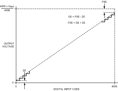 Figure 1. Input / Output Transfer Characteristic
 Figure 2. Serial Timing Diagram
7.7 Typical Characteristics
VREF = VA, fSCL = 3.4 MHz, TA = 25°C, Input Code Range 48 to 4047, unless otherwise stated.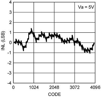 Figure 3. INL
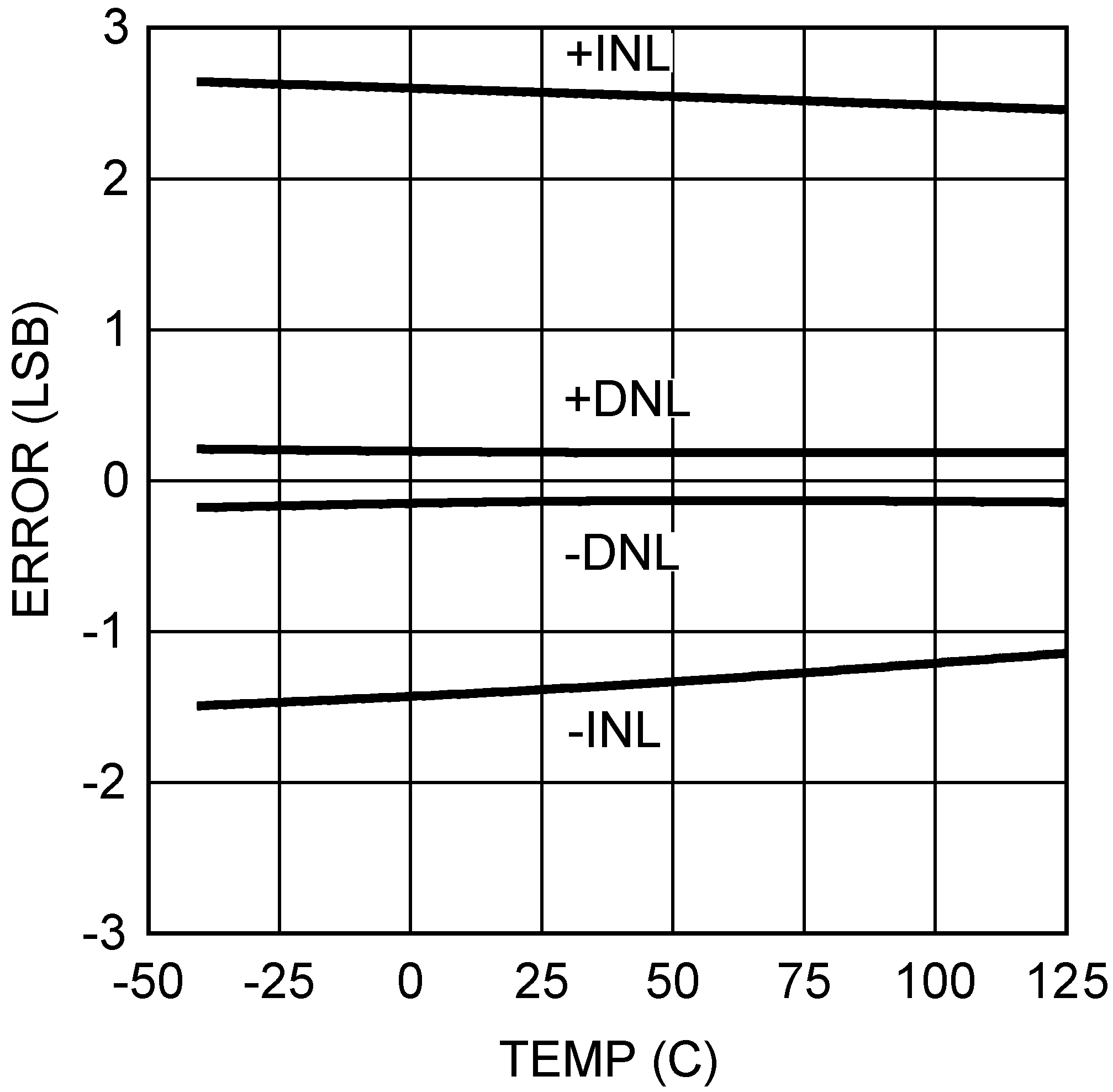 Figure 5. INL/DNL vs Temperature at VA = 3 V
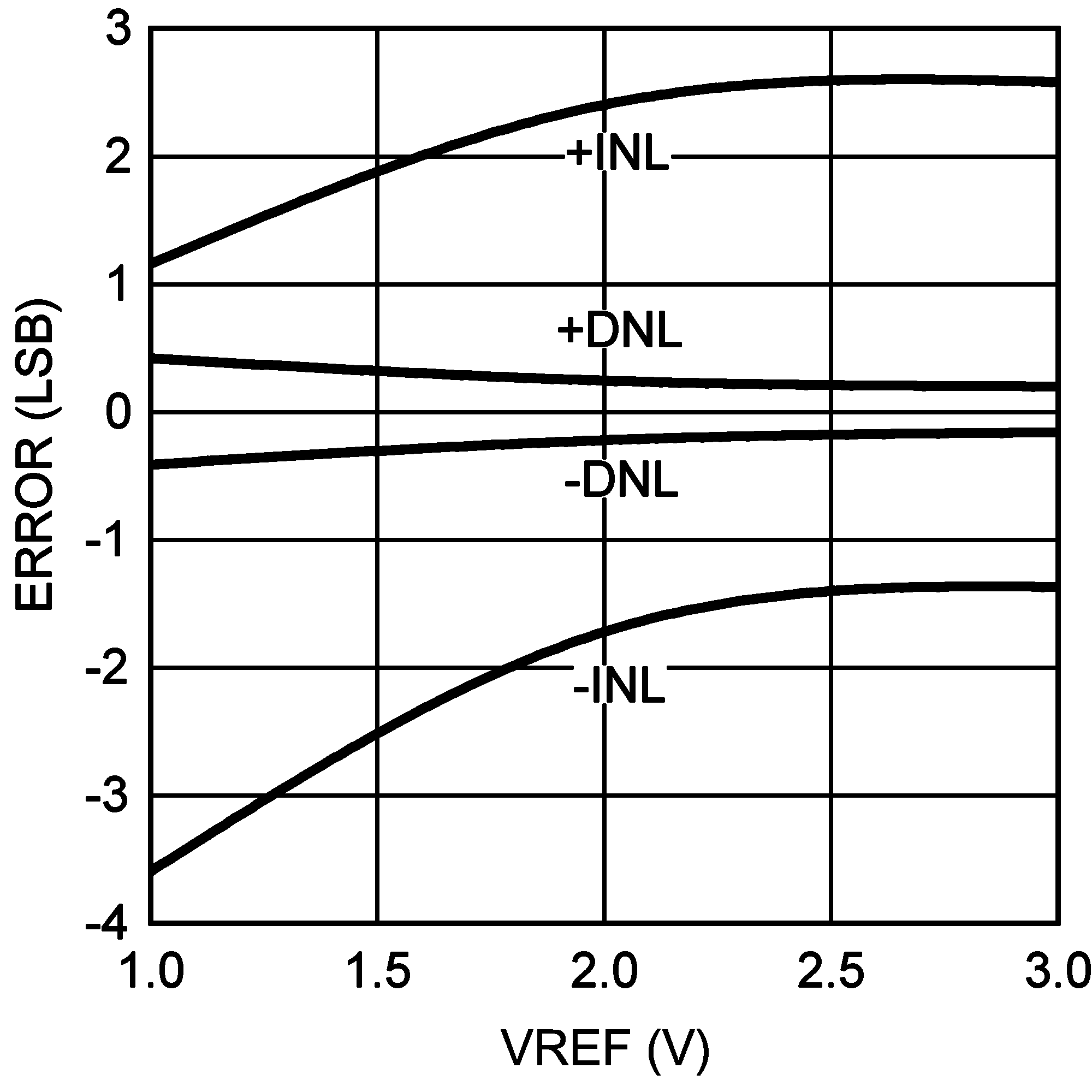 Figure 7. INL/DNL vs VREFIN at VA = 3 V
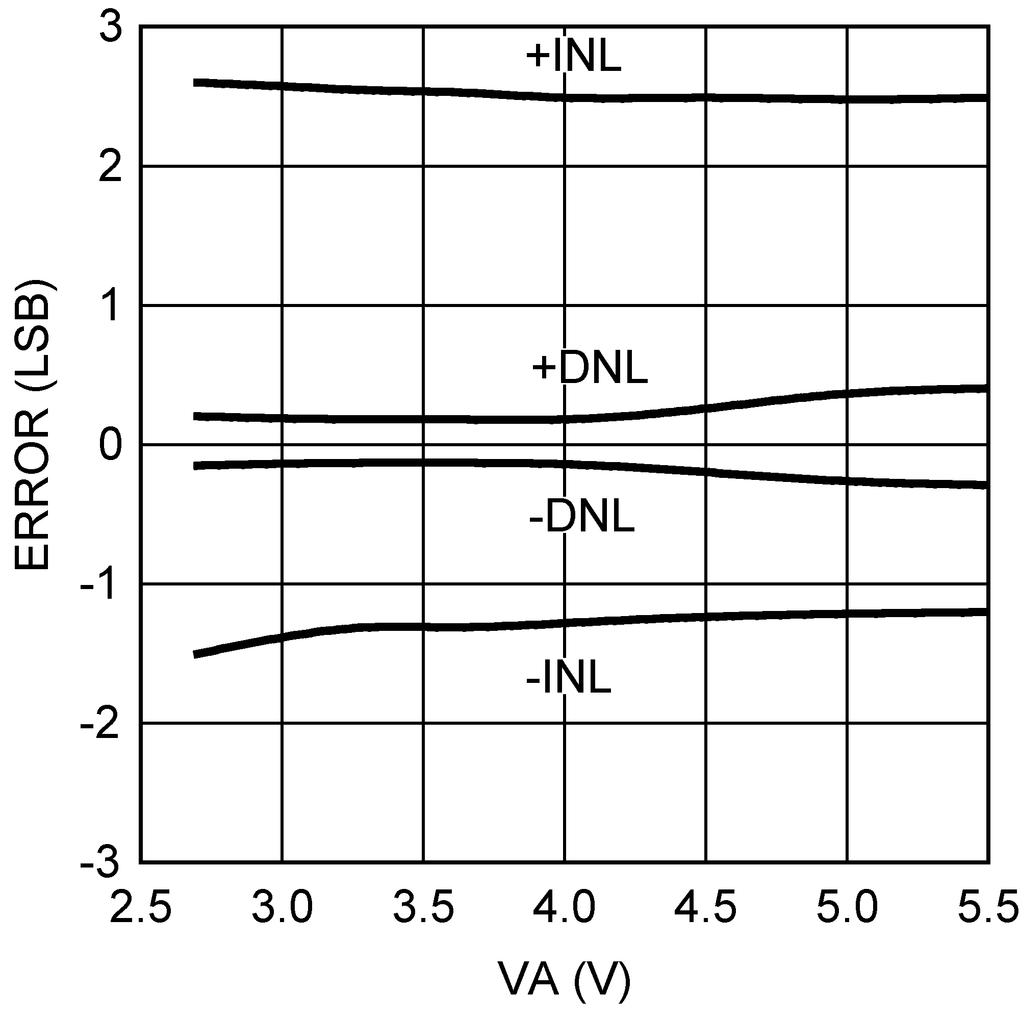 Figure 9. INL/DNL vs VA
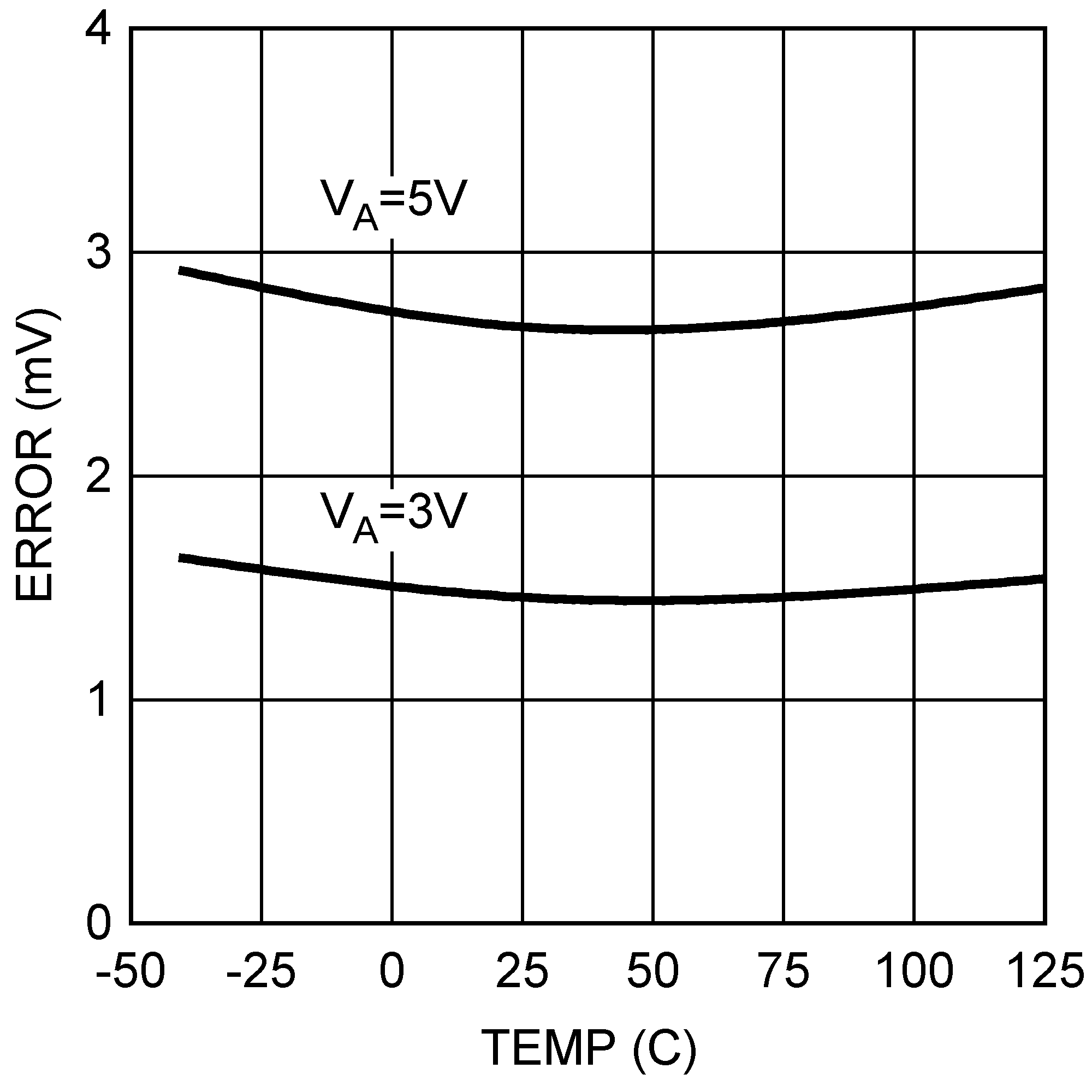 Figure 11. Zero Code Error vs Temperature
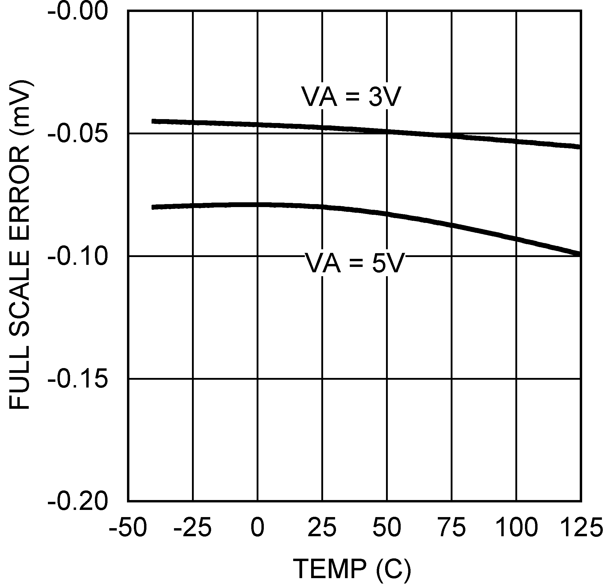 Figure 13. Full Scale Error vs Temperature
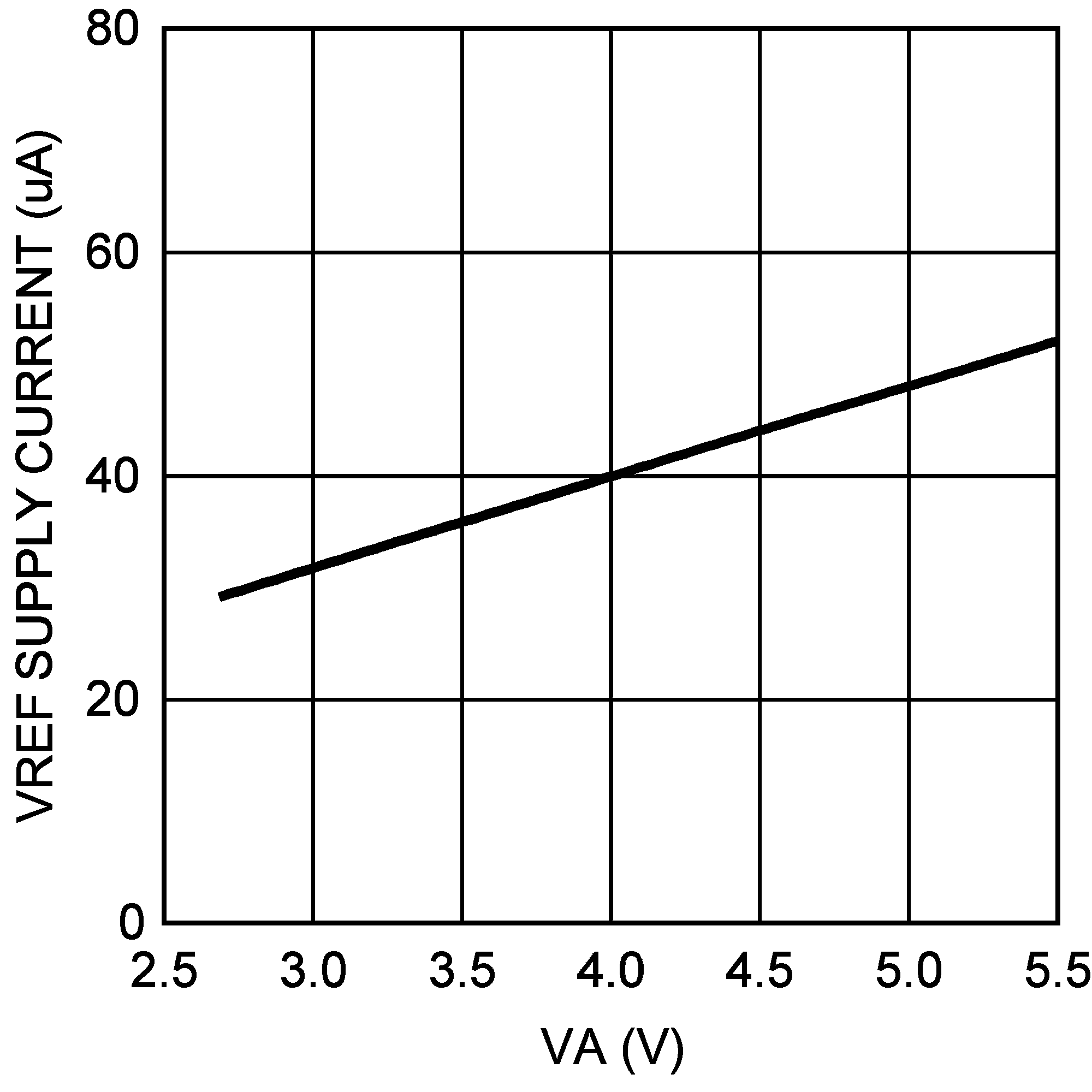 Figure 15. VREF Supply Current vs VA
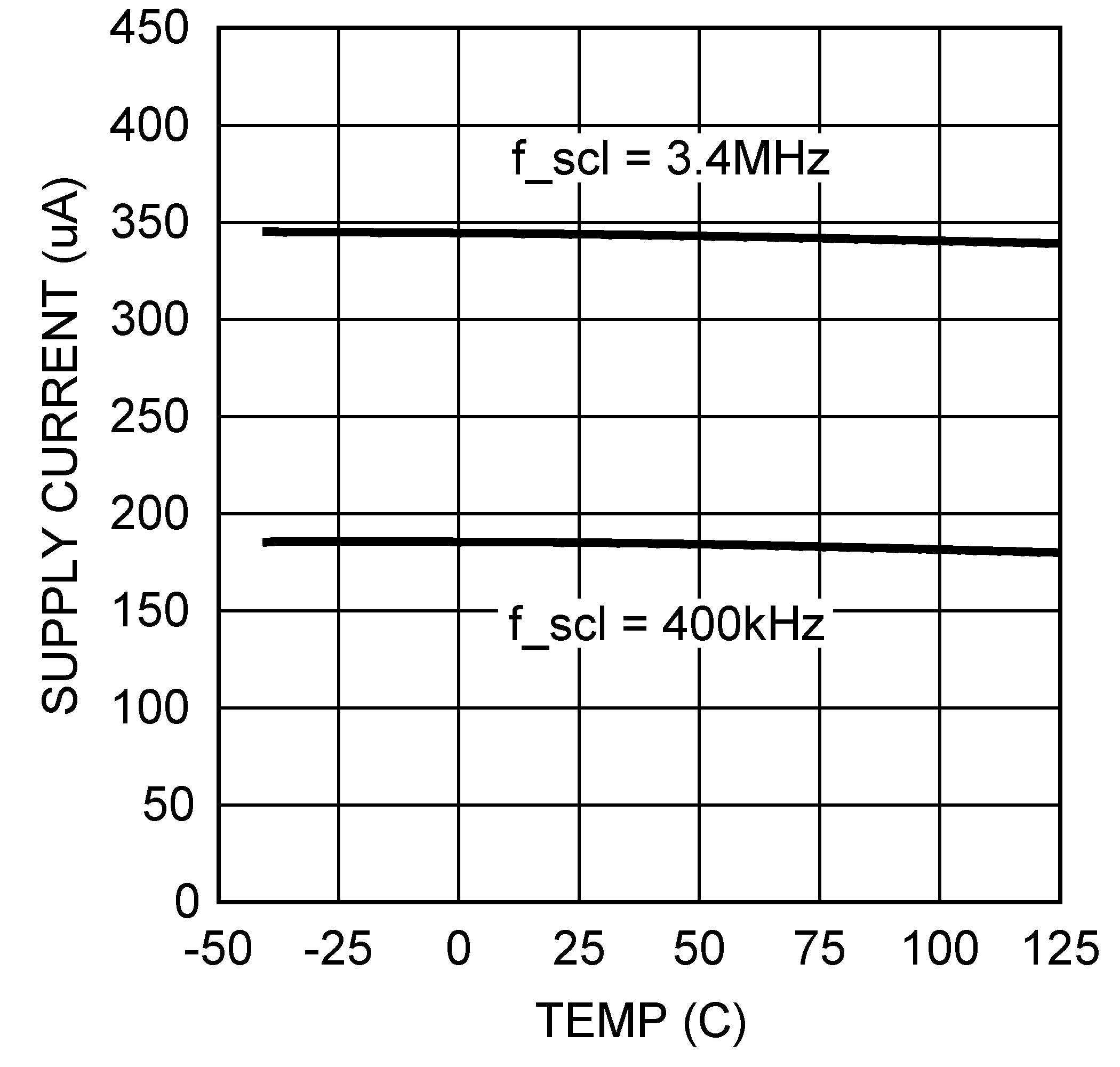 Figure 17. Total Supply Current vs Temperature at VA = 5 V
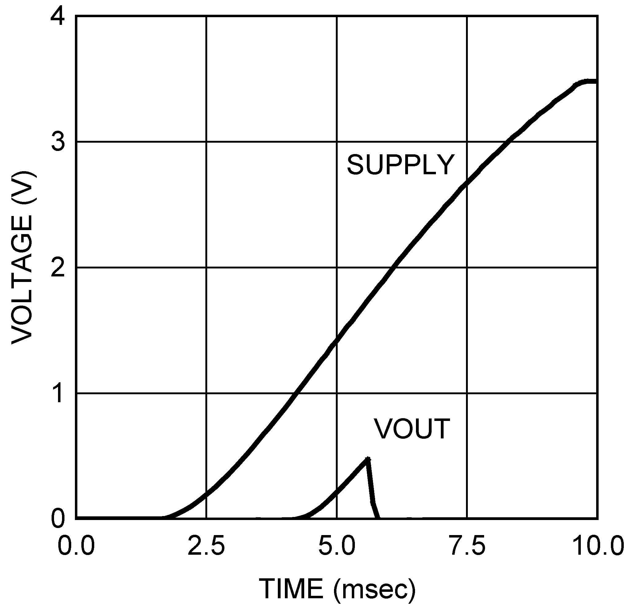 Figure 19. Power-On Reset
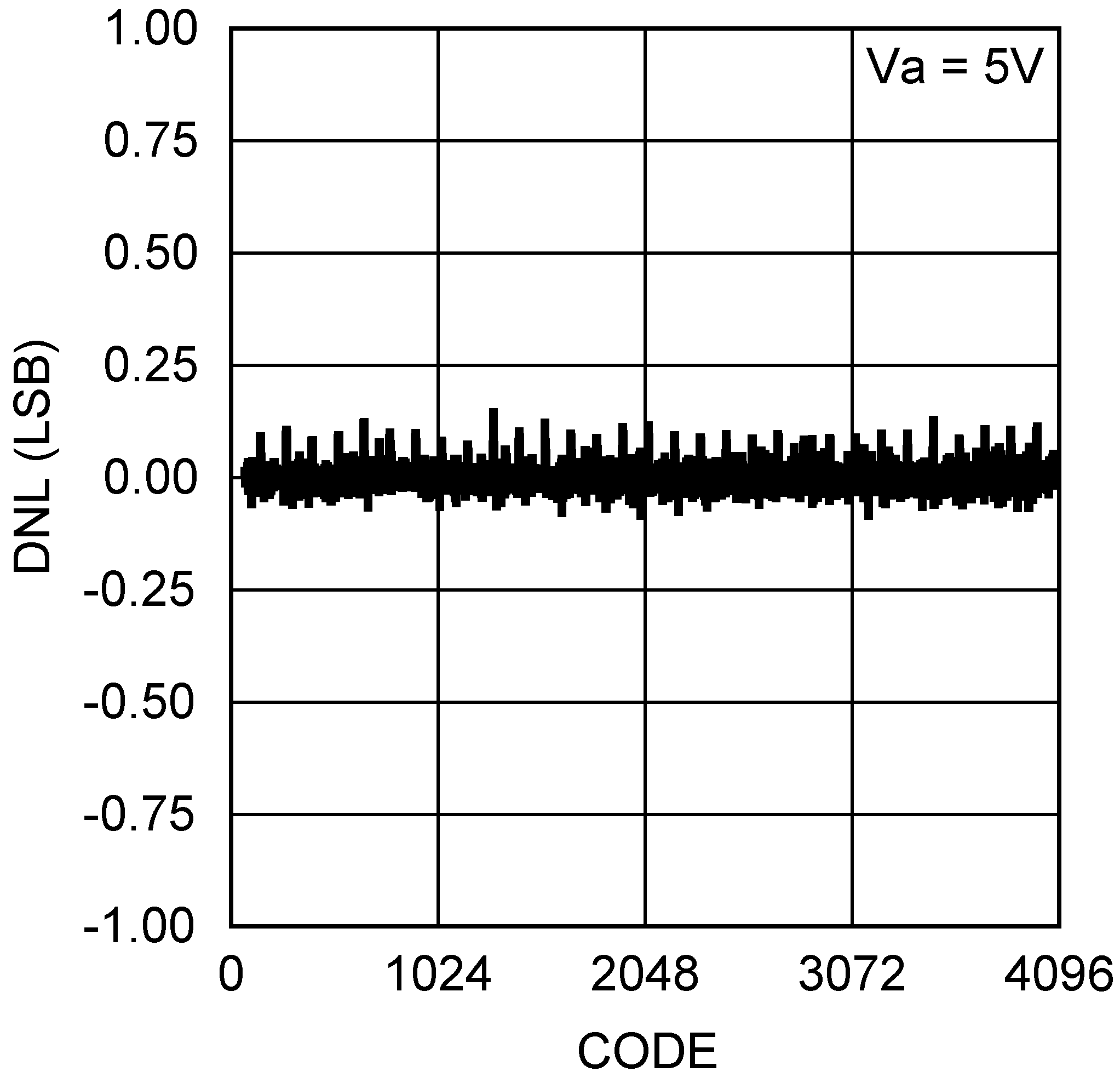 Figure 4. DNL
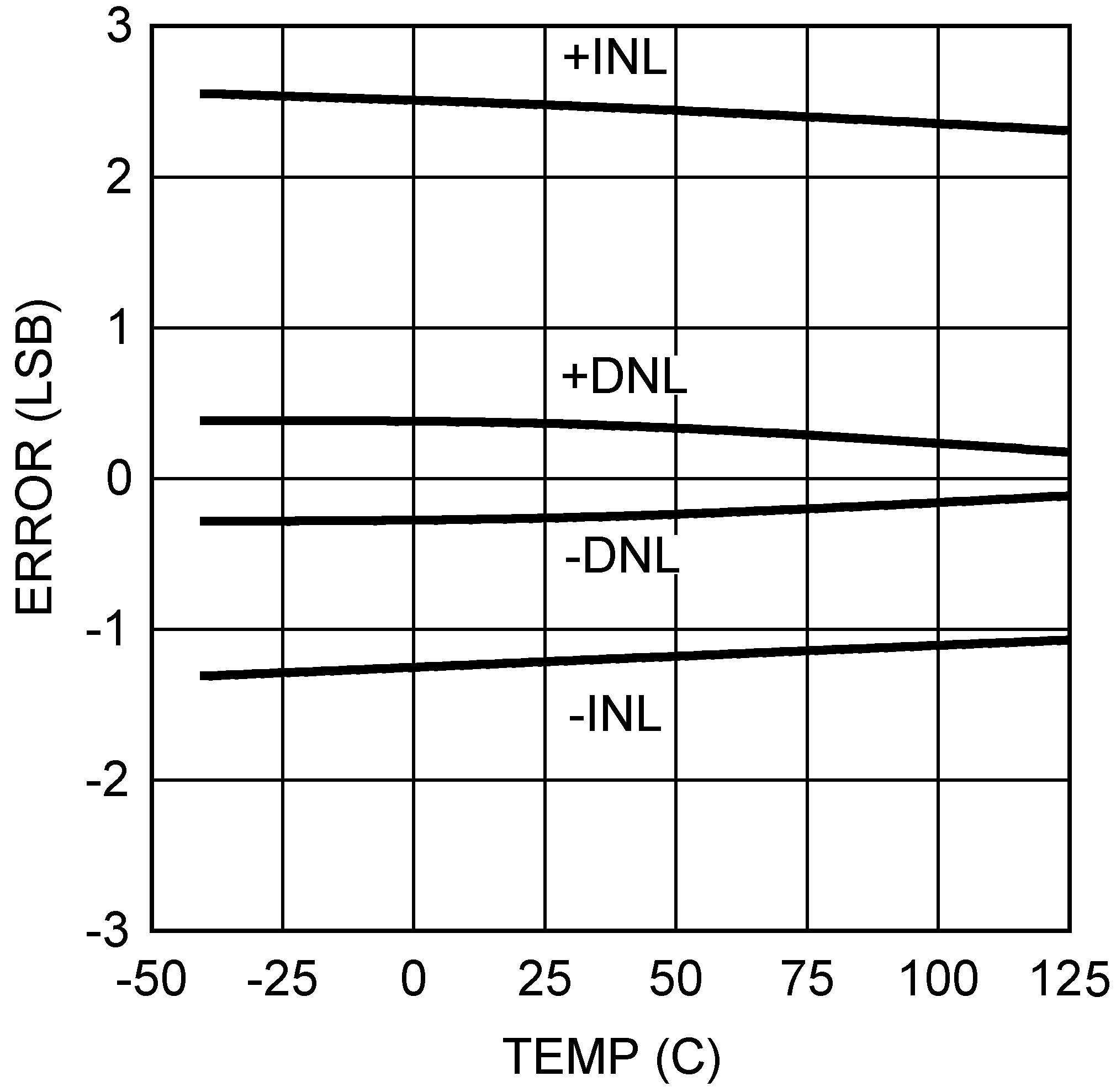 Figure 6. INL/DNL vs Temperature at VA = 5 V
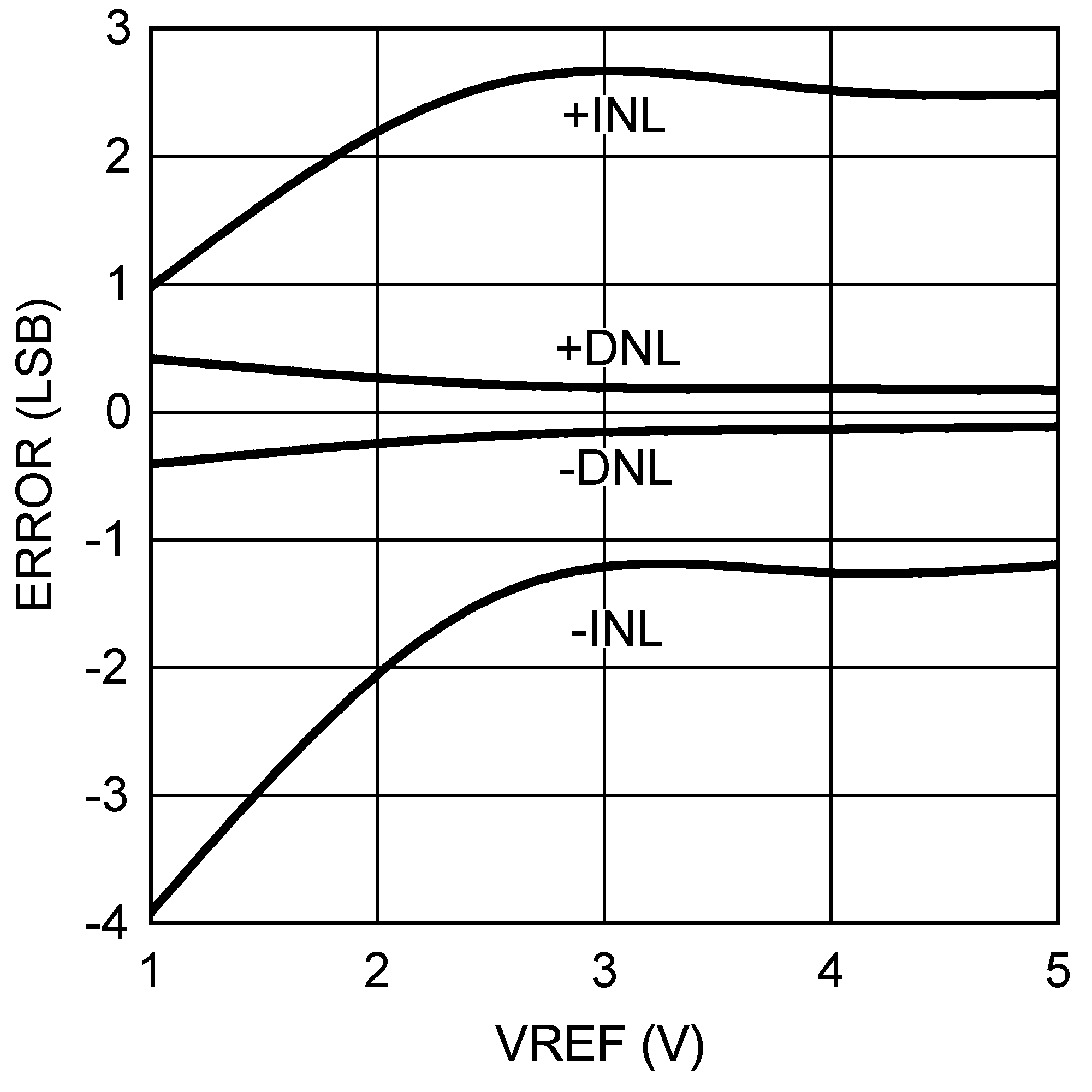 Figure 8. INL/DNL vs VREFIN at VA = 5 V
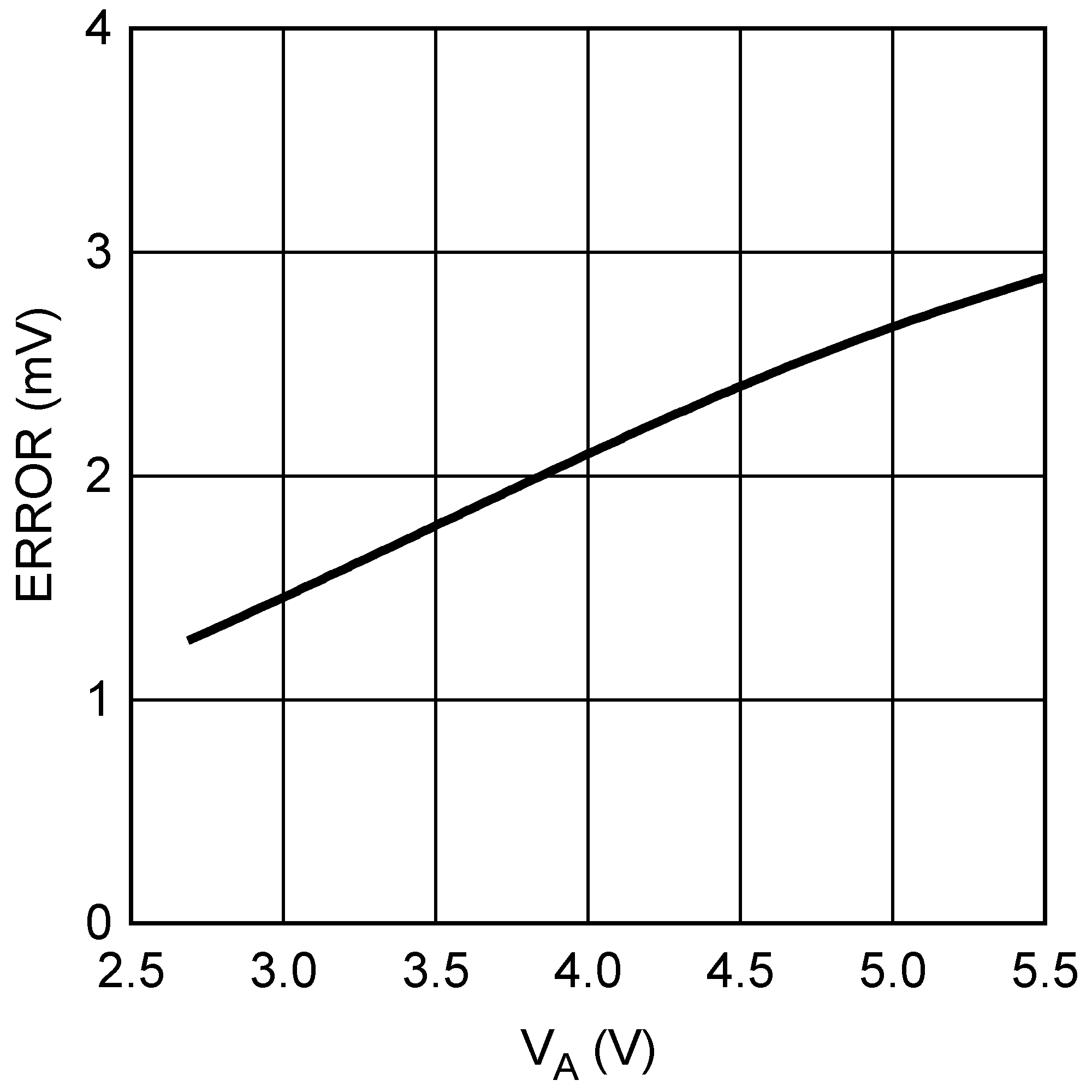 Figure 10. Zero Code Error vs VA
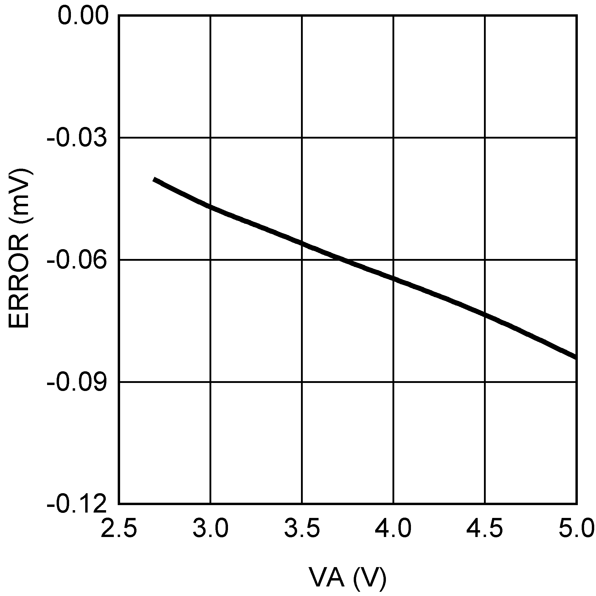 Figure 12. Full Scale Error vs VA
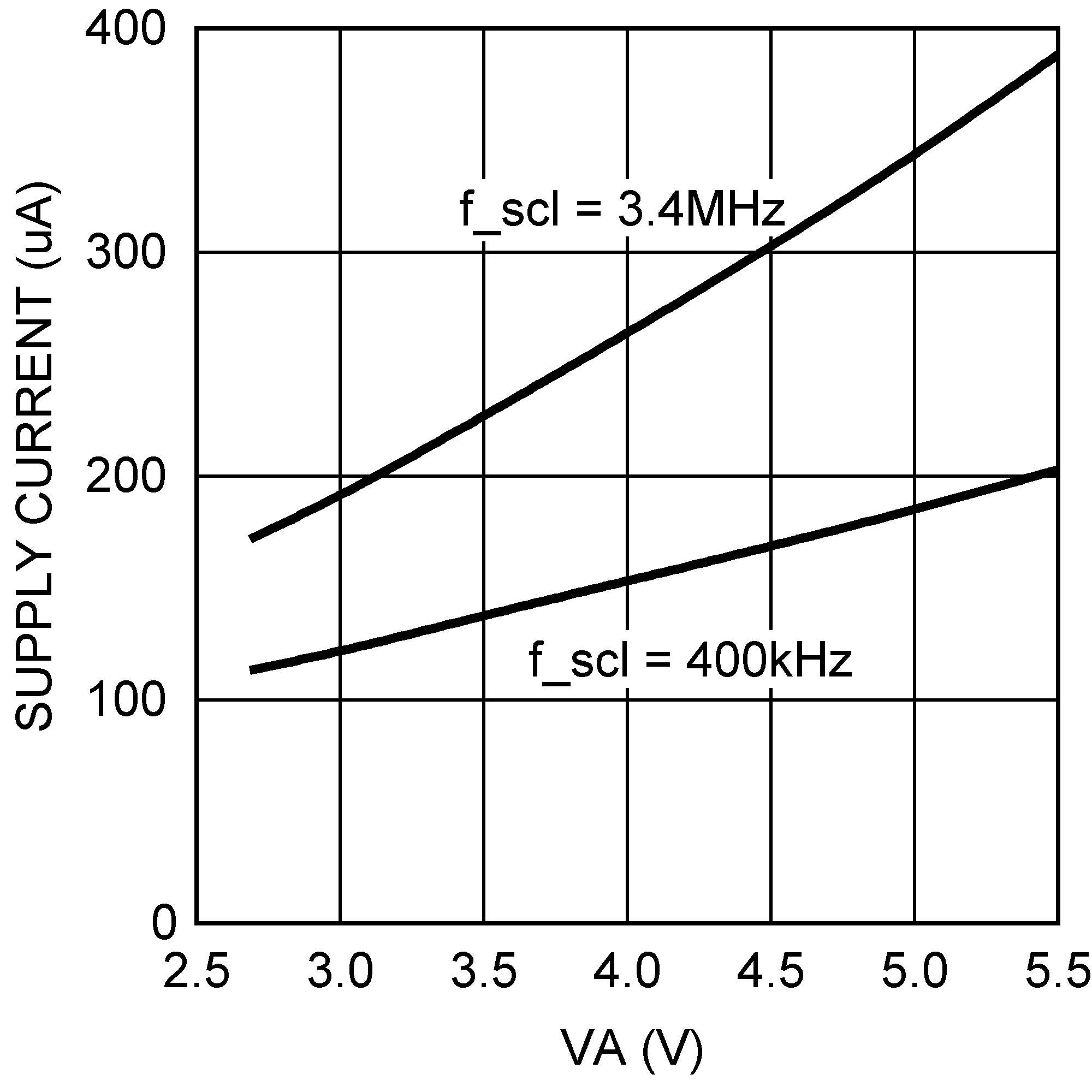 Figure 14. Total Supply Current vs VA
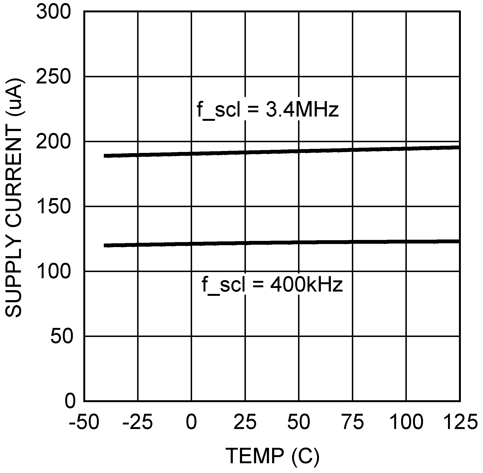 Figure 16. Total Supply Current vs Temperature at VA = 3 V
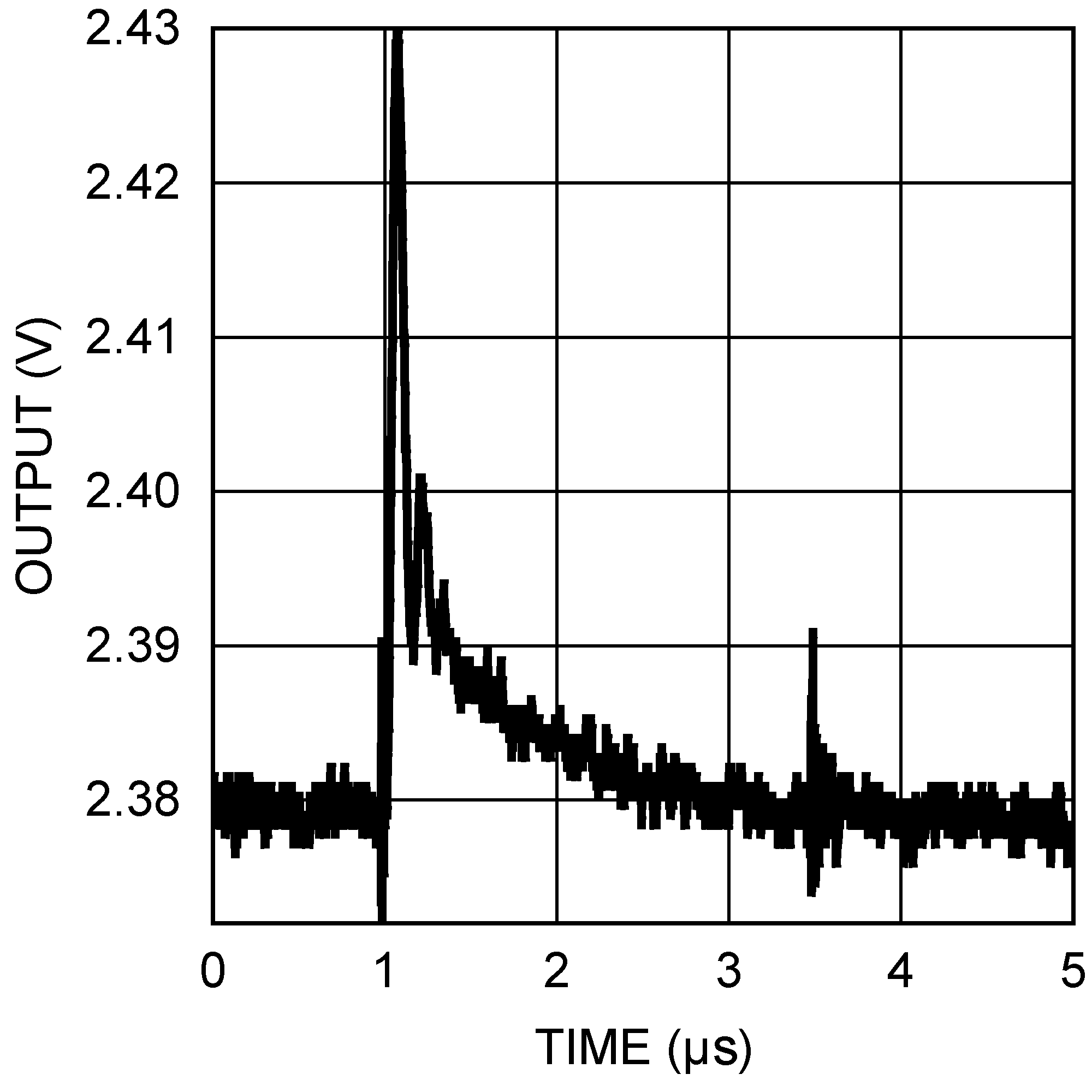 Figure 18. 5-V Glitch Response