SLASE16B January 2014 – May 2014 DAC37J82 , DAC38J82
PRODUCTION DATA.
- 1 Features
- 2 Applications
- 3 Description
- 4 Revision History
- 5 Pin Configuration and Functions
-
6 Specifications
- 6.1 Absolute Maximum Ratings
- 6.2 Handling Ratings
- 6.3 Recommended Operating Conditions
- 6.4 Thermal Information
- 6.5 DC Electrical Characteristics
- 6.6 Digital Electrical Characteristics
- 6.7 AC Electrical Characteristics
- 6.8 Timing Requirements
- 6.9 Switching Characteristics
- 6.10 Typical Characteristics
-
7 Detailed Description
- 7.1 Overview
- 7.2 Functional Block Diagram
- 7.3
Feature Description
- 7.3.1 Serdes Input
- 7.3.2 Serdes Rate
- 7.3.3 Serdes PLL
- 7.3.4 Serdes Equalizer
- 7.3.5 JESD204B Descrambler
- 7.3.6 JESD204B Frame Assembly
- 7.3.7 Serial Peripheral Interface (SPI)
- 7.3.8 Multi-Device Synchronization
- 7.3.9 Input Multiplexer
- 7.3.10 FIR Filters
- 7.3.11 Full Complex Mixer
- 7.3.12 Coarse Mixer
- 7.3.13 Dithering
- 7.3.14 Complex Summation
- 7.3.15 Quadrature Modulation Correction (QMC)
- 7.3.16 Group Delay Correction Block
- 7.3.17 Output Multiplexer
- 7.3.18 Power Measurement And Power Amplifier Protection
- 7.3.19 Serdes Test Modes
- 7.3.20 Error Counter
- 7.3.21 Eye Scan
- 7.3.22 JESD204B Pattern Test
- 7.3.23 Temperature Sensor
- 7.3.24 Alarm Monitoring
- 7.3.25 LVPECL Inputs
- 7.3.26 CMOS Digital Inputs
- 7.3.27 Reference Operation
- 7.3.28 Analog Outputs
- 7.3.29 DAC Transfer Function
- 7.4 Device Functional Modes
- 7.5 Register Map
- 8 Applications and Implementation
- 9 Power Supply Recommendations
- 10Layout
- 11Device and Documentation Support
- 12Mechanical, Packaging, and Orderable Information
6 Specifications
6.1 Absolute Maximum Ratings
over operating free-air temperature range (unless otherwise noted)(1)| MIN | MAX | UNIT | ||
|---|---|---|---|---|
| Supply voltage(2) | VDDDAC09, VDDDIG09 | –0.3 | 1.3 | V |
| VDDCLK09 | –0.3 | 1.3 | V | |
| VDDT09 | –0.3 | 1.3 | V | |
| VDDR18, VDDIO18, VDDS18, VQPS18 | –0.3 | 2.45 | V | |
| VDDAPLL18, VDDAREF18 | –0.3 | 2.45 | V | |
| VDDADAC33 | –0.3 | 4.0 | V | |
| Pin voltage(2) | RX[7..0]P/N | –0.5 V | VDDT09 + 0.5 V | V |
| SDENB, SCLK, SDIO, SDO, TXENA, ALARM, RESETB, SLEEP, TMS, TCLK, TDI, TDO, TRSTB, TESTMODE, SYNC_N_AB, SYNC_N_CD | –0.5 V | VDDIO18 + 0.5 V | V | |
| DACCLKP/N, SYSREFP/N | –0.5 V | VDDAPLL18 + 0.5 V | V | |
| SYNCBP/N | –0.5 V | VDDS18 + 0.5 V | V | |
| LPF | –0.5 V | VDDAPLL18 + 0.5 V | V | |
| IOUTAP/N, IOUTBP/N, IOUTCP/N, IOUTDP/N | –0.5 V | 1.0 V | V | |
| RBIAS, EXTIO, ATEST | –0.5 V | VDDAREF18 + 0.5 V | V | |
| IFORCE, VSENSE | –0.5 V | VDDDIG09 + 0.5 V | V | |
| AMUX1, AMUX0 | –0.5 V | VDDT09 + 0.5 V | V | |
| Peak input current (any input) | 20 | mA | ||
| Peak total input current (all inputs) | –30 | mA | ||
| Absolute maximum junction temperature TJ | 150 | °C | ||
| Operating free-air temperature range, TA: DAC37J82/DAC38J82 | –40 | 85 | °C | |
(1) Stresses beyond those listed under absolute maximum ratings may cause permanent damage to the device. These are stress ratings only and functional operation of these or any other conditions beyond those indicated under “recommended operating conditions” is not implied. Exposure to absolute-maximum-rated conditions for extended periods may affect device reliability.
(2) Measured with respect to GND.
6.2 Handling Ratings
| MIN | MAX | UNIT | ||
|---|---|---|---|---|
| Tstg | Storage temperature range | –65 | 150 | °C |
6.3 Recommended Operating Conditions
| MIN | NOM | MAX | UNIT | ||
|---|---|---|---|---|---|
| TJ | Recommended operating junction temperature(1) | 105 | °C | ||
| Maximum rated operating junction temperature | 125 | °C | |||
| TA | Recommended free-air temperature | -40 | 25 | 85 | °C |
(1) Prolonged use at this junction temperature may increase the device failure-in-time (FIT) rate.
6.4 Thermal Information
| THERMAL CONDUCTIVITY(1) | DAC3xJ82 | UNIT | |
|---|---|---|---|
| AAV (144 PINS) | |||
| RθJA | Theta junction-to-ambient (still air) | 31.4 | °C/W |
| RθJB | Theta junction-to-board | 12.6 | |
| RθJC | Theta junction-to-case, top | 1.8 | |
| ψJT | Psi junction-to-top of package | 0.2 | |
| ψJB | Psi junction-to-bottom of package | 12 | |
(1) Air flow or heat sinking reduces θJA and may be required for sustained operation at 85° and maximum operating conditions.
6.5 DC Electrical Characteristics
Typical values at TA = 25°C, full temperature range is TMIN = -40°C to TMAX = 85°C, nominal supplies, unless otherwise noted.| PARAMETER | TEST CONDITIONS | DAC37J82 | DAC38J82 | UNIT | |||||
|---|---|---|---|---|---|---|---|---|---|
| MIN | TYP | MAX | MIN | TYP | MAX | ||||
| Resolution | 16 | 16 | Bits | ||||||
| DC ACCURACY | |||||||||
| DNL | Differential nonlinearity | 1 LSB = IOUTFS/216 | ±4 | ±4 | LSB | ||||
| INL | Integral nonlinearity | ±6 | ±6 | LSB | |||||
| ANALOG OUTPUT | |||||||||
| Coarse gain linearity | ±0.04 | ±0.04 | LSB | ||||||
| Offset error | Mid code offset | ±0.001 | ±0.001 | %FSR | |||||
| Gain error | With external reference | ±2 | ±2 | %FSR | |||||
| With internal reference | ±2 | ±2 | |||||||
| Gain mismatch | With internal reference | ±2 | ±2 | %FSR | |||||
| Full scale output current | 20 | 30 | 20 | 30 | mA | ||||
| Output compliance range | –0.5 | 0.6 | –0.5 | 0.6 | V | ||||
| Output resistance | 300 | 300 | kΩ | ||||||
| Output capacitance | 5 | 5 | pF | ||||||
| REFERENCE OUTPUT | |||||||||
| VREF | Reference output voltage | 0.9 | 0.9 | V | |||||
| Reference output current(1) | 100 | 100 | nA | ||||||
| REFERENCE INPUT | |||||||||
| VEXTIO | Input voltage range | External reference mode | 0.1 | 0.9 | 1 | 0.1 | 0.9 | 1 | V |
| Input resistance | 1 | 1 | MΩ | ||||||
| Input capacitance | 50 | 50 | pF | ||||||
| TEMPERATURE COEFFICIENTS | |||||||||
| Offset drift | ±1 | ±1 | Ppm/°C | ||||||
| Gain drift | With external reference | ±15 | ±15 | ppm/°C | |||||
| With internal reference | ±30 | ±30 | |||||||
| Reference voltage drift | ±8 | ±8 | ppm/°C | ||||||
| POWER SUPPLY | |||||||||
| VDDADAC33 | 3.15 | 3.3 | 3.45 | 3.15 | 3.3 | 3.45 | V | ||
| VDDAPLL18, VDDAREF18, VDDS18, VQPS18, VDDR18 | 1.71 | 1.8 | 1.89 | 1.71 | 1.8 | 1.89 | V | ||
| VDDIO18 | 1.71 | 1.8 | 1.89 | 1.71 | 1.8 | 1.89 | V | ||
| VDDDIG09, VDDDAC09, VDDCLK09, VDDT09 | 0.85 | 0.9 | 0.95 | 0.85 | 0.9 | 0.95 | V | ||
| PSRR | Power Supply Rejection Ratio | DC tested | ±0.2 | ±0.2 | %FSR/V | ||||
| POWER CONSUMPTION | |||||||||
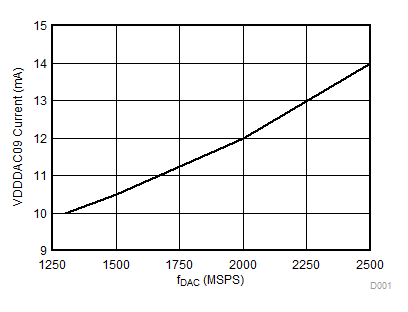
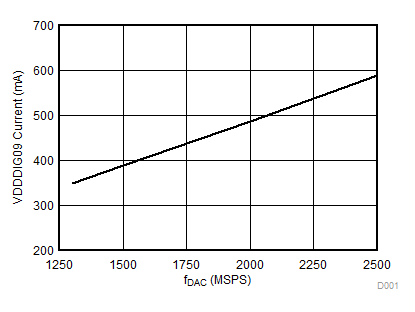
| I(VDDADAC33) | Analog supply current | MODE 1:(DAC38J82) fDAC=2.46GSPS, 2x interpolation, NCO on, QMC on, inverse sinc on, GDC off, PAP off, PLL on, LMF=421, SerDes rate = 12.3GSPS, 20mA FS output, IF=150MHz. |
- | 64 | 80 | mA | |||
| I(VDDDIG09) | Digital supply current | - | 628 | 800 | |||||
| I(VDDDAC09) | DAC supply current | - | 13 | 25 | |||||
| I(VDDCLK09) | Clock supply current | - | 86 | 120 | |||||
| I(VDDT09) | SerDes core supply current | - | 168 | 250 | |||||
| I(VDDR18) | SerDes analog supply current | - | 18 | 35 | |||||
| I(VDD18) | Other 1.8V supply current | - | 53 | 80 | |||||
| P | Power dissipation | - | 1144 | 1290(2) | mW | ||||
| I(VDDADAC33) | Analog supply current | MODE 2: (DAC37J82) fDAC=1.6GSPS, 2x interpolation, NCO on, QMC on, invsinc on, GDC off, PAP off, PLL on, LMF=421, SerDes rate = 8GSPS, 20mA FS output, IF=150MHz. |
64 | 64 | mA | ||||
| I(VDDDIG09) | Digital supply current | 418 | 418 | ||||||
| I(VDDDAC09) | DAC supply current | 10 | 10 | ||||||
| I(VDDCLK09) | Clock supply current | 57 | 57 | ||||||
| I(VDDT09) | SerDes core supply current | 139 | 139 | ||||||
| I(VDDR18) | SerDes analog supply current | 12 | 12 | ||||||
| I(VDD18) | Other 1.8V supply current | 50 | 50 | ||||||
| P | Power dissipation | 884 | 884 | mW | |||||
| I(VDDADAC33) | Analog supply current | MODE 3: fDAC=1.47456GSPS, 2x interpolation, NCO on, QMC off, invsinc off, GDC off, PAP off, PLL off, LMF=421, SerDes rate = 7.3728GSPS, 20mA FS output, IF=150MHz. |
64 | 64 | mA | ||||
| I(VDDDIG09) | Digital supply current | 363 | 363 | ||||||
| I(VDDDAC09) | DAC supply current | 10 | 10 | ||||||
| I(VDDCLK09) | Clock supply current | 50 | 50 | ||||||
| I(VDDT09) | SerDes core supply current | 135 | 135 | ||||||
| I(VDDR18) | SerDes analog supply current | 12 | 12 | ||||||
| I(VDD18) | Other 1.8V supply current | 30 | 30 | ||||||
| P | Power dissipation | 789 | 789 | mW | |||||
| I(VDDADAC33) | Analog supply current | MODE 4: fDAC=1.47456GSPS, 4x interpolation, NCO on, QMC off, invsinc off, GDC off, PAP off, PLL off, LMF=222, SerDes rate = 7.3728GSPS, 20mA FS output, IF=150MHz. |
64 | 64 | mA | ||||
| I(VDDDIG09) | Digital supply current | 312 | 312 | ||||||
| I(VDDDAC09) | DAC supply current | 10 | 10 | ||||||
| I(VDDCLK09) | Clock supply current | 50 | 50 | ||||||
| I(VDDT09) | SerDes core supply current | 76 | 76 | ||||||
| I(VDDR18) | SerDes analog supply current | 12 | 12 | ||||||
| I(VDD18) | Other 1.8V supply current | 30 | 30 | ||||||
| P | Power dissipation | 690 | 690 | mW | |||||
| I(VDDADAC33) | Analog supply current | MODE 5: fDAC=1.47456GSPS, x4, NCO off, QMC off, invsinc off, GDC off, PAP off, PLL off, LMF=222, SerDes rate = 7.3728GSPS, DAC output in sleep mode. |
13 | 13 | mA | ||||
| I(VDDDIG09) | Digital supply current | 263 | 263 | ||||||
| I(VDDDAC09) | DAC supply current | 8 | 8 | ||||||
| I(VDDCLK09) | Clock supply current | 50 | 50 | ||||||
| I(VDDT09) | SerDes core supply current | 76 | 76 | ||||||
| I(VDDR18) | SerDes analog supply current | 12 | 12 | ||||||
| I(VDD18) | Other 1.8V supply current | 26 | 26 | ||||||
| P | Power dissipation | 469 | 469 | mW | |||||
| I(VDDADAC33) | Analog supply current | MODE 6: fDAC=1000MSPS, 2x interpolation, NCO off, QMC off, invsinc off, GDC off, PAP off, PLL on, LMF=222, SerDes rate = 10GSPS, 20mA FS output, IF=150MHz. |
64 | 64 | mA | ||||
| I(VDDDIG09) | Digital supply current | 257 | 257 | ||||||
| I(VDDDAC09) | DAC supply current | 8 | 8 | ||||||
| I(VDDCLK09) | Clock supply current | 36 | 36 | ||||||
| I(VDDT09) | SerDes core supply current | 85 | 85 | ||||||
| I(VDDR18) | SerDes analog supply current | 15 | 15 | ||||||
| I(VDD18) | Other 1.8V supply current | 50 | 50 | ||||||
| P | Power dissipation | 676 | 676 | mW | |||||
| I(VDDADAC33) | Analog supply current | MODE 7: fDAC=1000MSPS, 2x interpolation, NCO off, QMC off invsinc off, GDC off, PAP off, PLL off, LMF=222, SerDes rate = 10GSPS, 20mA FS output, IF=150MHz. |
64 | 64 | mA | ||||
| I(VDDDIG09) | Digital supply current | 256 | 256 | ||||||
| I(VDDDAC09) | DAC supply current | 8 | 8 | ||||||
| I(VDDCLK09) | Clock supply current | 35 | 35 | ||||||
| I(VDDT09) | SerDes core supply current | 85 | 85 | ||||||
| I(VDDR18) | SerDes analog supply current | 15 | 15 | ||||||
| I(VDD18) | Other 1.8V supply current | 29 | 29 | ||||||
| P | Power dissipation | 636 | 636 | mW | |||||
| I(VDDADAC33) | Analog supply current | MODE 8: fDAC=625MSPS, 2x interpolation, NCO off, QMC off, invsinc off, GDC off, PAP off, PLL off, LMF=421, SerDes rate = 3.125GSPS, 20mA FS output, IF=20MHz. |
64 | 64 | mA | ||||
| I(VDDDIG09) | Digital supply current | 195 | 195 | ||||||
| I(VDDDAC09) | DAC supply current | 4 | 4 | ||||||
| I(VDDCLK09) | Clock supply current | 22 | 22 | ||||||
| I(VDDT09) | SerDes core supply current | 119 | 119 | ||||||
| I(VDDR18) | SerDes analog supply current | 11 | 11 | ||||||
| I(VDD18) | Other 1.8V supply current | 25 | 25 | ||||||
| P | Power dissipation | 582 | 582 | mW | |||||
| I(VDDADAC33) | Analog supply current | MODE 9: fDAC=1.23GSPS, no interpolation, NCO off, QMC off, invsinc off, GDC off, PAP off, PLL off, LMF=421, SerDes rate = 12.3GSPS, 20mA FS output, IF=150MHz; |
64 | 64 | mA | ||||
| I(VDDDIG09) | Digital supply current | 311 | 311 | ||||||
| I(VDDDAC09) | DAC supply current | 10 | 10 | ||||||
| I(VDDCLK09) | Clock supply current | 42 | 42 | ||||||
| I(VDDT09) | SerDes core supply current | 165 | 165 | ||||||
| I(VDDR18) | SerDes analog supply current | 18 | 18 | ||||||
| I(VDD18) | Other 1.8V supply current | 29 | 29 | ||||||
| P | Power dissipation | 771 | 771 | mW | |||||
| I(VDDADAC33) | Analog supply current | MODE 10: Power down mode, no clock, DAC in sleep mode, SerDes in sleep mode |
5 | 5 | mA | ||||
| I(VDDDIG09) | Digital supply current | 76 | 76 | ||||||
| I(VDDDAC09) | DAC supply current | 1 | 1 | ||||||
| I(VDDCLK09) | Clock supply current | 1 | 1 | ||||||
| I(VDDT09) | SerDes core supply current | 9 | 9 | ||||||
| I(VDDR18) | SerDes analog supply current | 0 | 0 | ||||||
| I(VDD18) | Other 1.8V supply current | 10 | 10 | ||||||
| P | Power dissipation | 112 | 112 | mW | |||||
(1) Use an external buffer amplifier with high impedance input to drive any external load.
(2) The MAX power limit is set separately which is NOT equal to the power consumption when all of the power supplies are at the MAX current.
6.6 Digital Electrical Characteristics
Typical values at TA = 25°C, full temperature range is TMIN = –40°C to TMAX = 85°C, nominal supplies, unless otherwise noted.| PARAMETER | TEST CONDITIONS | DAC37J82 | DAC38J82 | UNIT | ||||||
|---|---|---|---|---|---|---|---|---|---|---|
| MIN | TYP | MAX | MIN | TYP | MAX | |||||
| CML SERDES INPUTS: RX[7:0]P/N | ||||||||||
| VDIFF | Receiver input amplitude | 50 | 1200 | 50 | 1200 | mV | ||||
| VCOM | Input common mode (TERM=111) | 600 | 600 | mV | ||||||
| Input common mode (TERM=001) | 700 | 700 | ||||||||
| Input common mode (TERM=100) | 0 | 0 | ||||||||
| Input common mode (TERM=101) | 250 | 250 | ||||||||
| ZDIFF | Internal differential termination | 85 | 100 | 115 | 85 | 100 | 115 | Ω | ||
| fDATA | Serdes bit rate | 0.78125 | 12.5 | 0.78125 | 12.5 | Gbps | ||||
| LVPECL INPUTS: SYSREFP/N | ||||||||||
| VCOM | Input common mode voltage | 0.5 | 0.5 | V | ||||||
| VIDPP | Differential input peak-to-peak voltage | 400 | 800 | 400 | 800 | mV | ||||
| ZT | Internal termination | 100 | 100 | Ω | ||||||
| CL | Input capacitance | 2 | 2 | pF | ||||||
| LVPECL INPUTS: DACCLKP/N | ||||||||||
| VCOM | Input common mode voltage | 0.5 | 0.5 | V | ||||||
| VIDPP | Differential input peak-to-peak voltage | 400 | 800 | 400 | 800 | mV | ||||
| ZT | Internal termination | 100 | 100 | Ω | ||||||
| CL | Input capacitance | 2 | 2 | pF | ||||||
| Duty cycle | 40% | 60% | 40% | 60% | ||||||
| fDACCLK | DACCLKP/N Input Frequency | 1.6 | 2.5 | GHz | ||||||
| LVDS OUTPUTS: SYNCBP/N | ||||||||||
| VCOM | Output common mode voltage | 1.2 | 1.2 | V | ||||||
| ZT | Internal termination | 100 | 100 | Ω | ||||||
| VOD | Differential output voltage swing | 0.5 | 0.5 | V | ||||||
| CMOS INTERFACE: SDENB, SCLK, SDIO, SDO, TXENA, ALARM, RESETB, SLEEP, TMS, TCLK, TDI, TDO, TRSTB, TESTMODE, SYNC_N_AB, SYNC_N_CD | ||||||||||
| VIH | High-level input voltage | 0.7 x VDDIO18 | 0.7 x VDDIO18 | V | ||||||
| VIL | Low-level input voltage | 0.3 x VDDIO18 | 0.3 x VDDIO18 | V | ||||||
| IIH | High-level input current | -40 | 40 | -40 | 40 | µA | ||||
| IIL | Low-level input current | -40 | 40 | -40 | 40 | µA | ||||
| CI | CMOS Input capacitance | 2 | 2 | pF | ||||||
| VOH | ALARM, SDO, SDIO, TDO | Iload =–100 μA | VDDIO18 – 0.2 | VDDIO18 – 0.2 | V | |||||
| Iload = –2 mA | 0.8 x VDDIO18 | 0.8 x VDDIO18 | ||||||||
| VOL | ALARM, SDO, SDIO, TDO | Iload = 100 μA | 0.2 | 0.2 | V | |||||
| Iload = 2 mA | 0.5 | 0.5 | ||||||||
| PHASE LOCKED LOOP | ||||||||||
| PLL/VCO operating frequency | pll_vcosel = '1', pll_vco = '010001'(17), pll_vcoitune = '10', VCO Frequency = 3932.16MHz | Assured | Assured | |||||||
| pll_vcosel = '1', pll_vco = '011111'(31), pll_vcoitune = '10', VCO Frequency = 4120MHz | Assured | Assured | ||||||||
| pll_vcosel = '1', pll_vco = '110010'(50), pll_vcoitune = '10', VCO Frequency = 4423.68MHz | Assured | Assured | ||||||||
| pll_vcosel = '0', pll_vco = '001101'(13), pll_vcoitune = '11', VCO Frequency = 4608MHz | Assured | Assured | ||||||||
| pll_vcosel = '0', pll_vco = '011010'(26), pll_vcoitune = '11', VCO Frequency = 4800MHz | Assured | Assured | ||||||||
| pll_vcosel = '0', pll_vco = '100001'(33), pll_vcoitune = '11', VCO Frequency = 4915.2MHz | Assured | Assured | ||||||||
| pll_vcosel = '0', pll_vco = '100110'(38), pll_vcoitune = '11', VCO Frequency = 5000MHz | Assured | Assured | ||||||||
6.7 AC Electrical Characteristics
Typical values at TA = 25°C, full temperature range is TMIN = –40°C to TMAX = 85°C, nominal supplies, unless otherwise noted.| PARAMETER | TEST CONDITIONS / COMMENTS | DAC37J82 | DAC38J82 | UNIT | |||||
|---|---|---|---|---|---|---|---|---|---|
| MIN | TYP | MAX | MIN | TYP | MAX | ||||
| ANALOG OUTPUT(1) | |||||||||
| fDAC | Maximum DAC rate | 4x or higher interpolation | 1600 | 2500 | MSPS | ||||
| 2x interpolation | 1600 | 2460 | |||||||
| 1x interpolation | 1230 | 1230 | |||||||
| Digital latency (F=2, 2x interpolation) |
No interpolation, FIFO off, Mixer off, QMC off, Inverse sinc off | 11 | 11 | DAC clock cycles | |||||
| 2x Interpolation | 83 | 83 | |||||||
| 4x Interpolation | 211 | 211 | |||||||
| 8x Interpolation | 483 | 483 | |||||||
| 16x Interpolation | 1051 | 1051 | |||||||
| NCO | 48 | 48 | |||||||
| QMC | 32 | 32 | |||||||
| Inverse Sinc | 36 | 36 | |||||||
| PA Protection (pap_dlylen_sel = "0") | 68 | 68 | |||||||
| Dithering | 0 | 0 | |||||||
| Complex Summation | 0 | 0 | |||||||
| Coarse Fractional Delay | 51 | 51 | |||||||
| Fine Fractional Delay | 52 | 52 | |||||||
| AC PERFORMANCE(2) | |||||||||
| SFDR | Spurious free dynamic (0 to fDAC/2) |
fDAC = 2.5 GSPS, fOUT = 20 MHz, 0 dBFS | - | 79 | dBc | ||||
| fDAC = 2.5 GSPS, fOUT = 70 MHz, 0dBFS | - | 78 | |||||||
| fDAC = 2.5 GSPS, fOUT = 150 MHz, 0 dBFS | - | 72 | |||||||
| fDAC = 2.5 GSPS, fOUT = 230 MHz, 0dBFS | - | 67 | |||||||
| fDAC = 2.5 GSPS, fOUT = 20 MHz, -12 dBFS | - | 79 | |||||||
| fDAC = 2.5 GSPS, fOUT = 70 MHz, –12dBFS | - | 75 | |||||||
| fDAC = 2.5 GSPS, fOUT = 150 MHz, -12 dBFS | - | 70 | |||||||
| fDAC = 2.5 GSPS, fOUT = 230 MHz, –12dBFS | - | 65 | |||||||
| fDAC = 1.6 GSPS, fOUT = 20 MHz, 0 dBFS | 81 | 81 | |||||||
| fDAC = 1.6 GSPS, fOUT = 70 MHz, 0 dBFS | 77 | 77 | |||||||
| fDAC = 1.6 GSPS, fOUT = 150 MHz, 0 dBFS | 72 | 72 | |||||||
| fDAC = 1.6 GSPS, fOUT = 230 MHz, 0 dBFS | 68 | 68 | |||||||
| fDAC = 1.6 GSPS, fOUT = 20 MHz, -12 dBFS | 76 | 76 | |||||||
| fDAC = 1.6 GSPS, fOUT = 70 MHz, –12 dBFS | 72 | 72 | |||||||
| fDAC = 1.6 GSPS, fOUT = 150 MHz, -12 dBFS | 67 | 67 | |||||||
| fDAC = 1.6 GSPS, fOUT = 230 MHz, –12 dBFS | 64 | 64 | |||||||
| IMD3 | Third-order two-tone intermodulation distortion Each tone at –6dBFS |
fDAC = 2.5 GSPS, fOUT = 70 ± 0.5 MHz | - | 83 | dBc | ||||
| fDAC = 2.5 GSPS, fOUT = 150 ± 0.5 MHz | - | 75 | |||||||
| fDAC = 2.5 GSPS, fOUT = 230 ± 0.5 MHz | - | 70 | |||||||
| fDAC = 2.0 GSPS, fOUT = 70 ± 0.5 MHz | - | 86 | |||||||
| fDAC = 2.0 GSPS, fOUT = 150 ± 0.5 MHz | - | 78 | |||||||
| fDAC = 2.0 GSPS, fOUT = 230 ± 0.5 MHz | - | 73 | |||||||
| fDAC = 1.6 GSPS, fOUT = 70 ± 0.5 MHz | 83 | 83 | |||||||
| fDAC = 1.6 GSPS, fOUT = 150 ± 0.5 MHz | 73 | 73 | |||||||
| fDAC = 1.6 GSPS, fOUT = 230 ± 0.5 MHz | 66 | 66 | |||||||
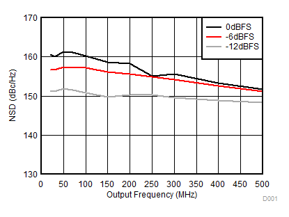
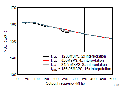
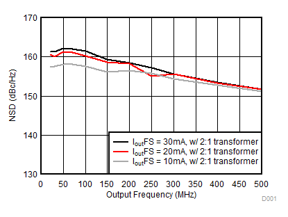
| NSD | Noise spectral density(2)
Tone at –6dBFS |
fDAC = 2.5 GSPS, fOUT = 70 MHz | - | -161 | dBFS/Hz | ||||
| fDAC = 2.5 GSPS, fOUT = 150 MHz | - | –159 | |||||||
| fDAC = 2.5 GSPS, fOUT = 230 MHz | - | -157 | |||||||
| fDAC = 2.0 GSPS, fOUT = 70 MHz | - | -161 | |||||||
| fDAC = 2.0 GSPS, fOUT = 150 MHz | - | -160 | |||||||
| fDAC = 2.0 GSPS, fOUT = 230 MHz | - | -158 | |||||||
| fDAC = 1.6 GSPS, fOUT = 70 MHz | -161 | -161 | |||||||
| fDAC = 1.6 GSPS, fOUT = 150 MHz | -159 | -159 | |||||||
| fDAC = 1.6 GSPS, fOUT = 230 MHz | -157 | -157 | |||||||
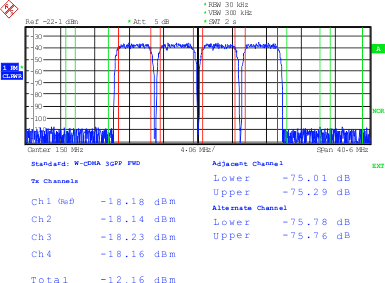
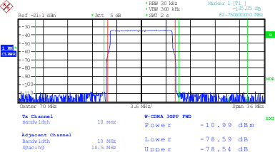
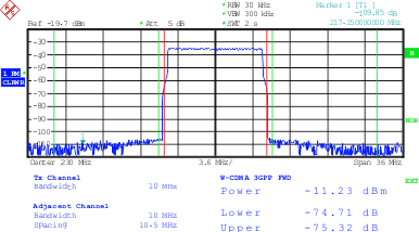
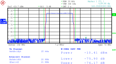
| ACLR(3) | Adjacent channel leakage ratio, single carrier | fDAC = 2.4576 GSPS, fOUT = 70 MHz | - | 82 | dBc | ||||
| fDAC = 2.4576 GSPS, fOUT = 150 MHz | - | 80 | |||||||
| fDAC = 2.4576 GSPS, fOUT = 230 MHz | - | 78 | |||||||
| fDAC = 1.96608 GSPS, fOUT = 70 MHz | - | 82 | |||||||
| fDAC = 1.96608 GSPS, fOUT = 150 MHz | - | 80 | |||||||
| fDAC = 1.96608 GSPS, fOUT = 230 MHz | - | 77 | |||||||
| fDAC = 1.47456 GSPS, fOUT = 70 MHz | 82 | 82 | |||||||
| fDAC = 1.47456 GSPS, fOUT = 150 MHz | 80 | 80 | |||||||
| fDAC = 1.47456 GSPS, fOUT = 230 MHz | 76 | 76 | |||||||
| Channel isolation | fDAC = 2.5 GSPS, fOUT = 20 MHz | - | 93 | dBc | |||||
| fDAC = 1.6 GSPS, fOUT = 20 MHz | 93 | 93 | |||||||
(1) Measured single ended into 50 Ω load.
(2) 2:1 transformer output termination, 50 Ω doubly terminated load.
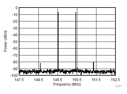
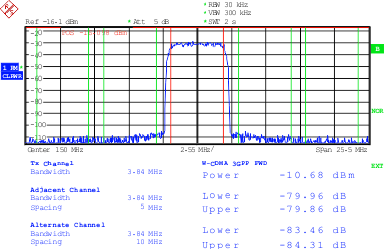
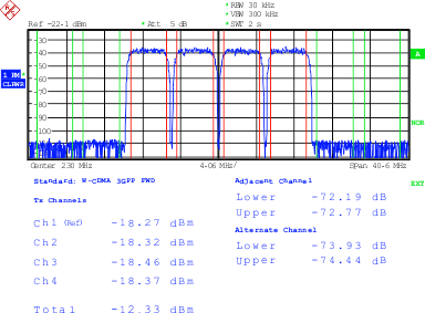
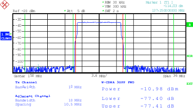
(3) Single carrier, W-CDMA with 3.84 MHz BW, 5-MHz spacing, centered at IF. TESTMODEL 1, 10 ms
6.8 Timing Requirements
Typical values at TA = 25°C, full temperature range is TMIN = –40°C to TMAX = 85°C, nominal supplies, unless otherwise noted.| PARAMETER | TEST CONDITIONS | DAC37J82 | DAC38J82 | UNIT | ||||||
|---|---|---|---|---|---|---|---|---|---|---|
| MIN | TYP | MAX | MIN | TYP | MAX | |||||
| DIGITAL INPUT TIMING SPECIFICATIONS | ||||||||||
| TIMING SYSREF INPUT: DACCLKP/N RISING EDGE LATCHING | ||||||||||
| ts(SYSREF) | Setup time, SYSREFP/N valid to rising edge of DACCLKP/N | 50 | 50 | ps | ||||||
| th(SYSREF) | Hold time, SYSREF/N valid after rising edge of DACCLKP/N | 50 | 50 | ps | ||||||
| TIMING SERIAL PORT | ||||||||||
| ts(SDENB) | Setup time, SDENB to rising edge of SCLK | 20 | 20 | ns | ||||||
| ts(SDIO) | Setup time, SDIO valid to rising edge of SCLK | 10 | 10 | ns | ||||||
| th(SDIO) | Hold time, SDIO valid to rising edge of SCLK | 5 | 5 | ns | ||||||
| t(SCLK) | Period of SCLK | Register config7 read (temperature sensor read) |
1 | 1 | µs | |||||
| All other registers | 100 | 100 | ns | |||||||
| td(Data) | Data output delay after falling edge of SCLK | 10 | 10 | ns | ||||||
| tRESET | Minimum RESETB pulsewidth | 25 | 25 | ns | ||||||
| ANALOG OUTPUT(1) | ||||||||||
| ts(DAC) | Output settling time to 0.1% | Transition: Code 0x0000 to 0xFFFF | 10 | 10 | ns | |||||
| Power-up Time | DAC wake-up time | IOUT current settling to 1% of IOUTFS from deep sleep | 90 | 90 | µs | |||||
| DAC sleep time | IOUT current settling to less than 1% of IOUTFS in deep sleep | 90 | 90 | |||||||
(1) Measured single ended into 50 Ω load.
6.9 Switching Characteristics
Typical values at TA = 25°C, full temperature range is TMIN = –40°C to TMAX = 85°C, nominal supplies, unless otherwise noted.| PARAMETER | TEST CONDITIONS | DAC37J82 | DAC38J82 | UNIT | |||||
|---|---|---|---|---|---|---|---|---|---|
| MIN | TYP | MAX | MIN | TYP | MAX | ||||
| ANALOG OUTPUT(1) | |||||||||
| tpd | Output propagation delay | DAC outputs are updated on the falling edge of DAC clock. Does not include Digital Latency (see below). | 2 | 2 | ns | ||||
| tr(IOUT) | Output rise time 10% to 90% | 50 | 50 | ps | |||||
| tf(IOUT) | Output fall time 90% to 10% | 50 | 50 | ps | |||||
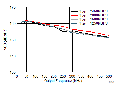
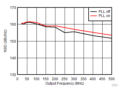
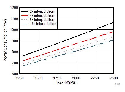
6.10 Typical Characteristics
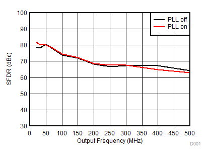
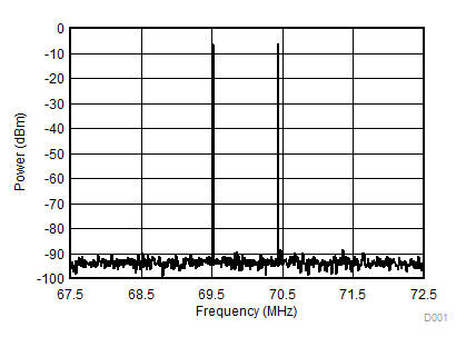
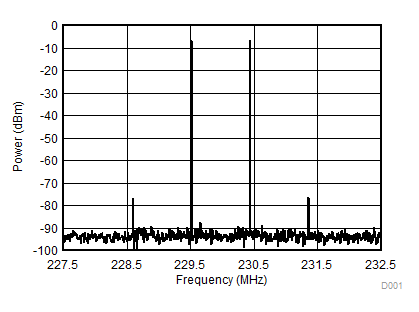
Unless otherwise noted, all plots are at TA = 25°C, nominal supply voltages, fDAC = 2460MSPS, 2x interpolation, 0dBFS digital input, 20mA full scale output current with 2:1 transformer, LMF = 421 and PLL is disabled.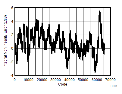 Figure 1. Integral Nonlinearity
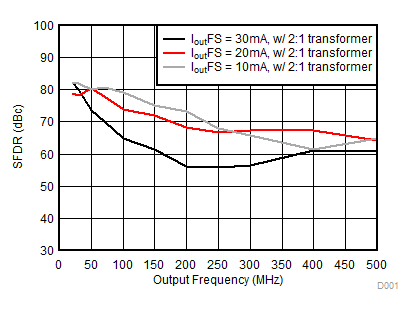
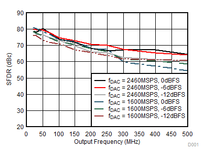 Figure 3. SFDR vs Output Frequency Over Input Scale
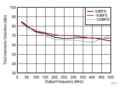 Figure 5. Third Harmonic Distortion vs Output Frequency Over Input Scale
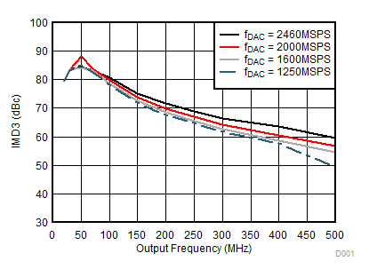
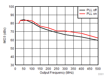
| fref = fDAC/4, M = 32, N = 8, Prescaler = 2 for PLL On |

| IF = 150MHz |
A.
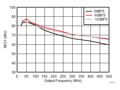
Figure 13. IMD3 vs Output Frequency Over Input Scale
| fref = fDAC/4, M = 32, N = 8, Prescaler = 2 for PLL On |
| IF = 150MHz, Tone Spacing = 1MHz |
| fref = fDAC/4, M = 32, N = 8, Prescaler = 2 for PLL On |
| Single Carrier WCDMA |
| Single Carrier WCDMA; fref = fDAC/4, M = 32, N = 8, Prescaler = 2 for PLL On |
| QMC On, CMIX On, NCO On |
| QMC Off, CMIX Off, NCO Off |
| QMC On, CMIX On, NCO On |

| IF = 70MHz |

| IF = 230MHz | ||
| IF = 150MHz |
| IF = 70MHz | ||
| IF = 230MHz | ||
| IF = 150MHz | ||
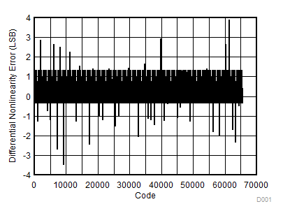 Figure 2. Differential Nonlinearity
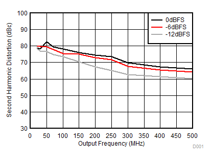 Figure 4. Second Harmonic Distortion vs Output Frequency Over Input Scale
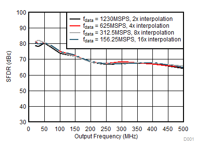 Figure 6. SFDR vs Output Frequency Over Interpolation
| IF = 70MHz |
| IF = 230MHz |
| IF = 70MHz, Tone Spacing = 1MHz |
| IF = 230MHz, Tone Spacing = 1MHz |
| Single Carrier WCDMA |
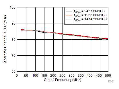
Single Carrier WCDMA; fref = fDAC/4, M = 32, N = 8, Prescaler = 2 for PLL On
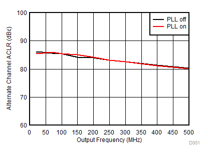
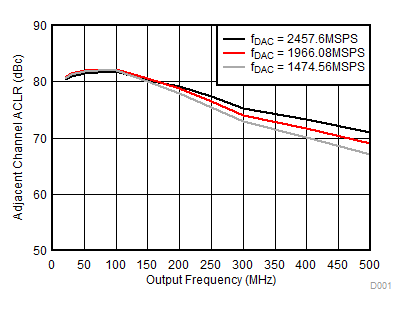
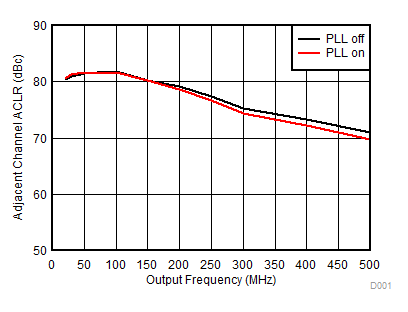
Figure 28. ACLR (Adjacent Channel) vs Output Frequency Over Clocking Options
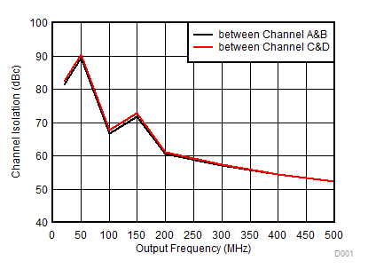
| Between Channel AB pair and CD pair | ||
| QMC Off, CMIX Off, NCO Off |
| QMC On, CMIX On, NCO On |
| IF = 150MHz |

| IF = 70MHz |
| IF = 230MHz |
| IF = 150MHz | ||
| IF = 70MHz | ||
| IF = 230MHz | ||