JAJS137I NOVEMBER 2006 – November 2016 DCH010505D , DCH010505S , DCH010512D , DCH010512S , DCH010515D , DCH010515S
PRODUCTION DATA.
- 1 特長
- 2 アプリケーション
- 3 概要
- 4 改訂履歴
- 5 Device Comparison Tables
- 6 Pin Configuration and Functions
- 7 Specifications
- 8 Detailed Description
- 9 Application and Implementation
- 10Power Supply Recommendations
- 11Layout
- 12デバイスおよびドキュメントのサポート
- 13メカニカル、パッケージ、および注文情報
9 Application and Implementation
NOTE
Information in the following applications sections is not part of the TI component specification, and TI does not warrant its accuracy or completeness. TI’s customers are responsible for determining suitability of components for their purposes. Customers should validate and test their design implementation to confirm system functionality.
9.1 Application Information
9.1.1 Optional Input and Output Filters
DCH01 power modules include internal input and output ceramic capacitors in all their designs. However, some applications require much lower levels of either input reflected or output ripple or noise. This application note describes various filters and design techniques found to be successful in reducing both input and output ripple or noise.
9.1.1.1 Input and Output Capacitors
The easiest way to reduce output ripple and noise is to add 1 or more ceramic capacitors each with a value of 4.7-µF or greater. Ceramic capacitors must be placed close to the output power terminals. A single 4.7-µF ceramic capacitor reduces the output ripple or noise by 10% to 30%.
Switching regulators draw current from the input line in pulses at their operating frequency. The amount of reflected (input) ripple or noise generated is directly proportional to the equivalent source impedance of the power source including the impedance of any input lines. The addition of a 4.7-µF ceramic capacitor, near the input power pins, reduces reflected conducted ripple or noise by 30% to 50%.
The recommended maximum capacitive load on the output of the DCH01 is 100 µF (non-ceramic).
9.1.1.2 π Filters
If a further reduction in ripple or noise level is required for an application, higher order filters must be used. A π (pi) filter, employing a ferrite bead inductor in series with the input or output terminals of the regulator reduces the ripple or noise by at least 15-20 db (see Figure 22 and Figure 23). Ceramic capacitors are required for the inductor to be effective in reduction of ripple and noise.
These inductors plus ceramic capacitors form an excellent filter because of the rejection at the switching frequency. The placement of this filter is critical. It must be located as close as possible to the input or output pins to be efffective. The ferrite bead is small (5.1 mm x 3 mm), easy to use, low cost, and has low dc resistance. Fair-Rite manufactures a surface-mount bead (part number 2773019447) or through hole (part number 2673000701) rated to 5 A. Inductors with a value from 1 µH to 5 µH can be used in place of the ferrite bead inductor.
 Figure 22. DCH01 Series π Filter
 Figure 23. DCH01 Series π Filter (5 V at 1 W)
9.1.3 Connecting the DCH01 in Series
It is possible to connect the outputs of multiple DCH01s in series to provide non-standard voltage rails. The outputs of dual output DCH01 versions can also be connected in series to provide 2 × the magnitude of VO (as shown in Figure 25). For example, a dual 5-V DCH01 could be connected to provide a 10-V rail.
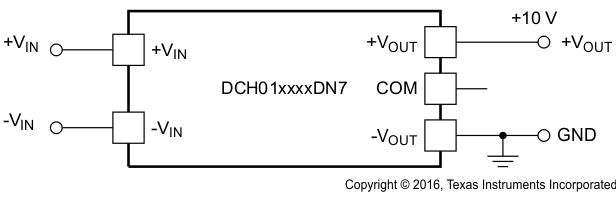 Figure 25. Connecting Dual Outputs in Series
9.1.4 Connecting the DCH01 in Parallel
If the output power from 1 DCH01 is not sufficient, it is possible to parallel the outputs of multiple DCH01s (as shown in Figure 26).
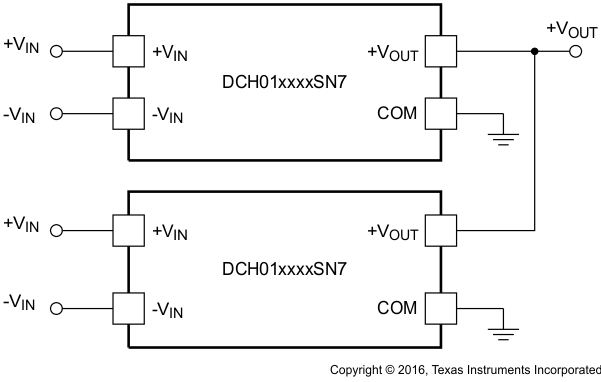 Figure 26. Connecting Multiple DCH01s in Parallel
9.2 Typical Application
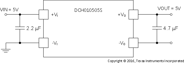 Figure 27. Typical Application Schematic
9.2.1 Design Requirements
For this design example, use the parameters listed in Table 3 and follow the procedures in Detailed Design Procedure.
Table 3. Design Example Parameters
| PARAMETER | VALUE | ||
|---|---|---|---|
| +VI | Input voltage | 5 V | |
| +VO | Output voltage | 5 V | |
| IOUT | Output current rating | 200 mA | |
9.2.2 Detailed Design Procedure
9.2.2.1 Input Capacitor
For any DCH01 design, select a 2.2-µF, low-ESR, ceramic input capacitor to ensure a good startup performance.
9.2.2.2 Output Capacitor
For any DCH01 design, select a 4.7-µF, low-ESR, ceramic output capacitor to reduce output ripple.
9.2.3 Application Curves
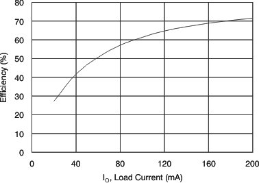
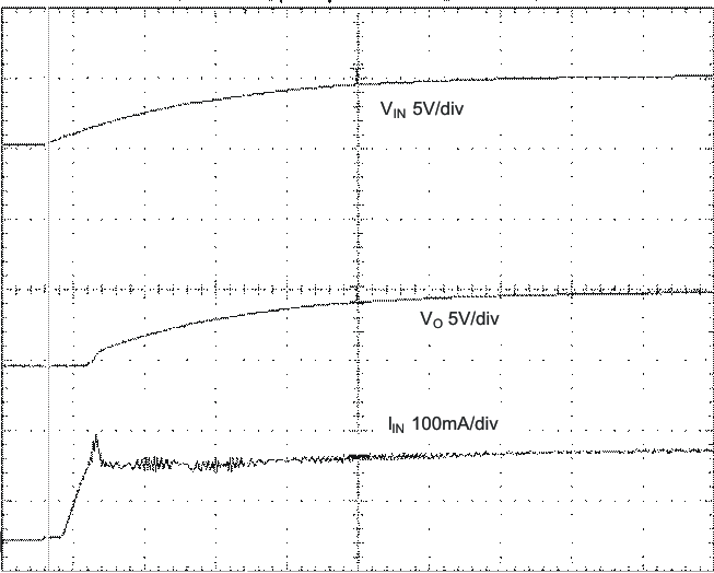 Figure 29. DCH010505 Startup Waveforms