JAJSH82A April 2019 – September 2019 DLP3034-Q1
PRODUCTION DATA.
- 1 特長
- 2 アプリケーション
- 3 概要
- 4 改訂履歴
- 5 Pin Configuration and Functions
-
6 Specifications
- 6.1 Absolute Maximum Ratings
- 6.2 Storage Conditions
- 6.3 ESD Ratings
- 6.4 Recommended Operating Conditions
- 6.5 Thermal Information
- 6.6 Electrical Characteristics
- 6.7 Timing Requirements
- 6.8 Switching Characteristics
- 6.9 System Mounting Interface Loads
- 6.10 Physical Characteristics of the Micromirror Array
- 6.11 Micromirror Array Optical Characteristics
- 6.12 Window Characteristics
- 6.13 Chipset Component Usage Specification
- 7 Detailed Description
- 8 Application and Implementation
- 9 Power Supply Recommendations
- 10Layout
- 11デバイスおよびドキュメントのサポート
- 12メカニカル、パッケージ、および注文情報
6.10 Physical Characteristics of the Micromirror Array
| PARAMETER | VALUE | UNIT | ||
|---|---|---|---|---|
| N | Number of active columns | See Figure 7 | 684 | micromirrors |
| M | Number of active rows | See Figure 7 | 608 | micromirrors |
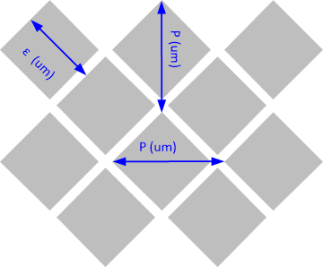
| ε | Micromirror (pixel) pitch – diagonal | See Figure 8 | 7.6 | µm |
| P | Micromirror (pixel) pitch – horizontal and vertical | See Figure 8 | 10.8 | µm |
| Micromirror active array width | P × M + P / 2; see Figure 7 | 6.5718 | mm | |
| Micromirror active array height | (P × N) / 2 + P / 2; see Figure 7 | 3.699 | mm | |
| Micromirror active border | Pond of micromirror (POM)(1) | 10 | micromirrors/side | |
(1) The structure and qualities of the border around the active array includes a band of partially functional micromirrors called the POM. These micromirrors are structurally and/or electrically prevented from tilting toward the bright or ON state, but still require an electrical bias to tilt toward OFF.
 Figure 8. Mirror (Pixel) Pitch