JAJSKY2A November 2017 – February 2023 DLP650LE
PRODUCTION DATA
- 1 特長
- 2 アプリケーション
- 3 概要
- 4 Revision History
- 5 Pin Configuration and Functions
-
6 Specifications
- 6.1 Absolute Maximum Ratings
- 6.2 Storage Conditions
- 6.3 ESD Ratings
- 6.4 Recommended Operating Conditions
- 6.5 Thermal Information
- 6.6 Electrical Characteristics
- 6.7 Capacitance at Recommended Operating Conditions
- 6.8 Timing Requirements
- 6.9 Window Characteristics
- 6.10 System Mounting Interface Loads
- 6.11 Micromirror Array Physical Characteristics
- 6.12 Micromirror Array Optical Characteristics
- 6.13 Chipset Component Usage Specification
- 7 Detailed Description
- 8 Application and Implementation
- 9 Power Supply Recommendations
- 10Device and Documentation Support
- 11Mechanical, Packaging, and Orderable Information
9.2 DMD Power Supply Power-Down Procedure
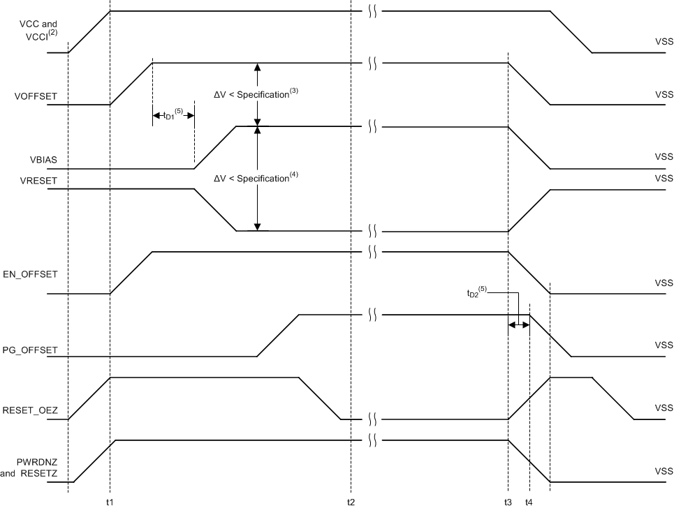
- During power-down, VCC and VCCI must be supplied until after VBIAS, VRESET, and VOFFSET are discharged to within the specified limit of ground. See Table 9-2.
- During power-down, it is a strict requirement that the voltage delta between VBIAS and VOFFSET must be within the specified limit shown in Section 6.4.
- During power-down, there is no requirement for the relative timing of VRESET with respect to VBIAS.
- Power supply slew rates during power-down are flexible, provided that the transient voltage levels follow the requirements specified in Section 6.1, in Section 6.4, and in Figure 9-1.
- During power-down, LVCMOS input pins must be less than specified in Section 6.4.
Table 9-1 DMD Power Supply Transition Points
| TIME | DESCRIPTION |
|---|---|
| t1 | DLP controller software enables the DMD power supplies to turn on after RESET_OEZ is at logic high |
| t1 | PG_OFFSET turns OFF after EN_OFFSET turns OFF per the tD2 specification in Table 9-2. |
| t2 | DLP controller software initiates the global VBIAS command. |
| t3 | After the DMD micromirror park sequence is complete, the DLP controller software initiates a hardware power-down that activates PWRDNZ and disables VBIAS, VRESET and VOFFSET. |
| t4 | Under power-loss conditions where emergency DMD micromirror park procedures are being enacted by the DLP controller hardware, EN_OFFSET may turn off after PG_OFFSET has turned off. The OEZ signal should go high prior to PG_OFFSET turning off to indicate the DMD micromirror has completed the emergency park procedures. |

- Not to scale. Some details omitted for clarity. See Section 6.4 for all specified limits and Section 5 table for pin descriptions.
- To prevent excess current, the supply voltage difference |VCCI – VCC| must be less than the specified limit.
- To prevent excess current, the supply voltage difference |VBIAS – VOFFSET| must be less than the specified limit.
- To prevent excess current, the supply voltage difference |VBIAS – VRESET| must be less than the specified limit.
- See Table 9-2 for delay time descriptions.
- See Table 9-1 for transition time point descriptions.
Table 9-2 Delay Times Requirements
| DELAY TIME | DESCRIPTION | MIN | NOM | MAX | UNIT |
|---|---|---|---|---|---|
| tD1 | Delay time period from VOFFSET settled at recommended operating voltage to VBIAS and VRESET power up. | 1 | 2 | ms | |
| tD2 | Delay time period between PG_OFFSET hold time and when EN_OFFSET goes low | 100 | ns |