JAJSHL4C March 2015 – June 2019 DLPC150
PRODUCTION DATA.
- 1 特長
- 2 アプリケーション
- 3 概要
- 4 改訂履歴
- 5 Pin Configuration and Functions
-
6 Specifications
- 6.1 Absolute Maximum Ratings
- 6.2 ESD Ratings
- 6.3 Recommended Operating Conditions
- 6.4 Thermal Information
- 6.5 Electrical Characteristics Over Recommended Operating Conditions
- 6.6 Electrical Characteristics
- 6.7 High-Speed Sub-LVDS Electrical Characteristics
- 6.8 Low-Speed SDR Electrical Characteristics
- 6.9 System Oscillators Timing Requirements
- 6.10 Power-Up and Reset Timing Requirements
- 6.11 Parallel Interface Frame Timing Requirements
- 6.12 Parallel Interface General Timing Requirements
- 6.13 Flash Interface Timing Requirements
- 7 Parameter Measurement Information
- 8 Detailed Description
- 9 Application and Implementation
- 10Power Supply Recommendations
-
11Layout
- 11.1
Layout Guidelines
- 11.1.1 PCB Layout Guidelines For Internal Controller PLL Power
- 11.1.2 DLPC150 Reference Clock
- 11.1.3 General PCB Recommendations
- 11.1.4 General Handling Guidelines for Unused CMOS-Type Pins
- 11.1.5 Maximum Pin-to-Pin, PCB Interconnects Etch Lengths
- 11.1.6 Number of Layer Changes
- 11.1.7 Stubs
- 11.1.8 Terminations
- 11.1.9 Routing Vias
- 11.2 Layout Example
- 11.3 Thermal Considerations
- 11.1
Layout Guidelines
- 12デバイスおよびドキュメントのサポート
- 13メカニカル、パッケージ、および注文情報
6.8 Low-Speed SDR Electrical Characteristics
over operating free-air temperature range (unless otherwise noted)| PARAMETER | ID | TEST CONDITIONS | MIN | MAX | UNIT |
|---|---|---|---|---|---|
| Operating voltage | VCC18 (all signal groups) | 1.64 | 1.96 | V | |
| DC input high voltage | VIHD(DC)
Signal group 1 |
All | 0.7 × VCC18 | VCC18 + 0.5 | V |
| DC input low voltage(5) | VILD(DC)
Signal group 1 |
All | –0.5 | 0.3 × VCC18 | V |
| AC input high voltage(4) | VIHD(AC)
Signal group 1 |
All | 0.8 × VCC18 | VCC18 + 0.5 | V |
| AC input low voltage | VILD(AC)
Signal group 1 |
All | –0.5 | 0.2 × VCC18 | V |
| Slew rate (1)(2)(3)(6) | Signal group 1 | 1 | 3 | V/ns | |
| Signal group 2 | 0.25 | ||||
| Signal group 3 | 0.5 | ||||
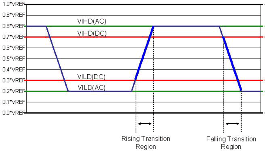
(1) Signal group 1 output slew rate for rising edge is measured between VILD(DC) to VIHD(AC).
(2) Signal group 1 output slew rate for falling edge is measured between VIHD(DC) to VILD(AC).
(3) Signal group 1: See Figure 2.
(4) VIHD(AC) max applies to overshoot.
(5) VILD(AC) min applies to undershoot.
(6) Signal groups 2 and 3 output slew rate for rising edge is measured between VILD(AC) to VIHD(AC).
 Figure 2. Low Speed (Ls) I/O Input Thresholds