JAJSHL4C March 2015 – June 2019 DLPC150
PRODUCTION DATA.
- 1 特長
- 2 アプリケーション
- 3 概要
- 4 改訂履歴
- 5 Pin Configuration and Functions
-
6 Specifications
- 6.1 Absolute Maximum Ratings
- 6.2 ESD Ratings
- 6.3 Recommended Operating Conditions
- 6.4 Thermal Information
- 6.5 Electrical Characteristics Over Recommended Operating Conditions
- 6.6 Electrical Characteristics
- 6.7 High-Speed Sub-LVDS Electrical Characteristics
- 6.8 Low-Speed SDR Electrical Characteristics
- 6.9 System Oscillators Timing Requirements
- 6.10 Power-Up and Reset Timing Requirements
- 6.11 Parallel Interface Frame Timing Requirements
- 6.12 Parallel Interface General Timing Requirements
- 6.13 Flash Interface Timing Requirements
- 7 Parameter Measurement Information
- 8 Detailed Description
- 9 Application and Implementation
- 10Power Supply Recommendations
-
11Layout
- 11.1
Layout Guidelines
- 11.1.1 PCB Layout Guidelines For Internal Controller PLL Power
- 11.1.2 DLPC150 Reference Clock
- 11.1.3 General PCB Recommendations
- 11.1.4 General Handling Guidelines for Unused CMOS-Type Pins
- 11.1.5 Maximum Pin-to-Pin, PCB Interconnects Etch Lengths
- 11.1.6 Number of Layer Changes
- 11.1.7 Stubs
- 11.1.8 Terminations
- 11.1.9 Routing Vias
- 11.2 Layout Example
- 11.3 Thermal Considerations
- 11.1
Layout Guidelines
- 12デバイスおよびドキュメントのサポート
- 13メカニカル、パッケージ、および注文情報
9.2 Typical Application
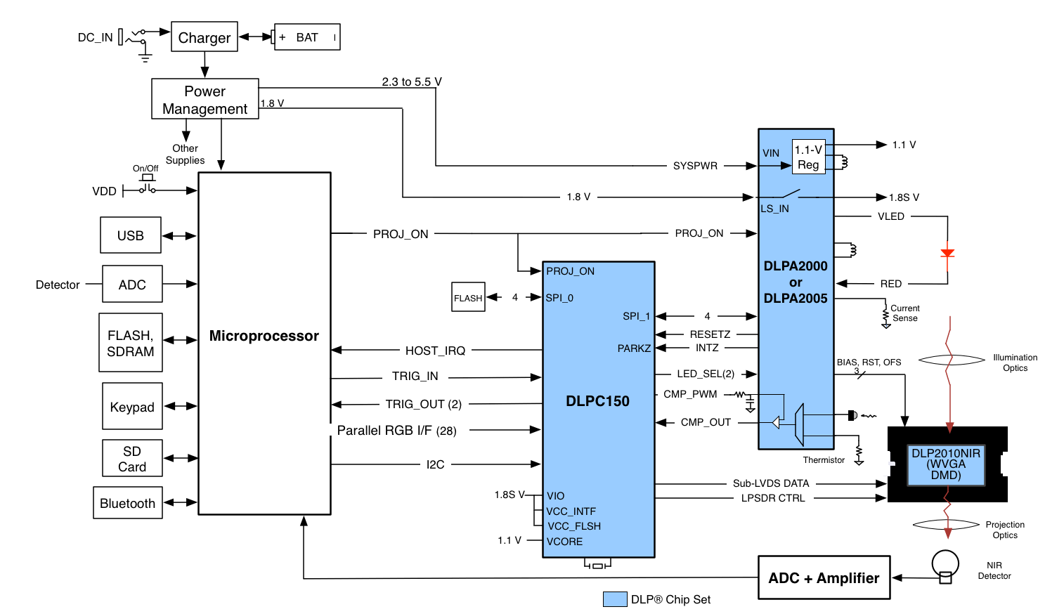
A typical embedded system application using the DLPC150 controller and the DLPC2010NIR is shown in Figure 13. In this configuration, the DLPC150 controller supports a 24-bit parallel RGB input, typical of LCD interfaces, from an external source or processor. The DLPC150 controller processes the digital input image and converts the data into the format needed by the DLP2010NIR. The DLP2010NIR steers light by setting specific micromirrors to the "on" position, directing light to the detector, while unwanted micromirrors are set to "off" position, directing light away from the detector. The microprocessor sends binary images to the DLP2010NIR to steer specific wavelengths of light into the detector. The microprocessor uses an analog-to-digital converter to sample the signal received by the detector into a digital value. By sequentially selecting different wavelengths of light and capturing the values at the detector, the microprocessor can then plot a spectral response to the light.
 Figure 13. Typical Application Diagram