JAJSEE9E January 2015 – May 2018 DRV10975
PRODUCTION DATA.
- 1 特長
- 2 アプリケーション
- 3 概要
- 4 改訂履歴
- 5 概要(続き)
- 6 Pin Configuration and Functions
- 7 Specifications
-
8 Detailed Description
- 8.1 Overview
- 8.2 Functional Block Diagram
- 8.3 Feature Description
- 8.4
Device Functional Modes
- 8.4.1 Motor Parameters
- 8.4.2 Starting the Motor Under Different Initial Conditions
- 8.4.3 Motor Start Sequence
- 8.4.4 Start-Up Current Setting
- 8.4.5 Closed Loop
- 8.4.6 Current Limit
- 8.4.7 Lock Detect and Fault Handling
- 8.4.8 AVS Function
- 8.4.9 PWM Output
- 8.4.10 FG Customized Configuration
- 8.4.11
Diagnostics and Visibility
- 8.4.11.1 Motor Status Readback
- 8.4.11.2 Motor Speed Readback
- 8.4.11.3 Motor Electrical Period Readback
- 8.4.11.4 BEMF Constant Readback
- 8.4.11.5 Motor Estimated Position by IPD
- 8.4.11.6 Supply Voltage Readback
- 8.4.11.7 Speed Command Readback
- 8.4.11.8 Speed Command Buffer Readback
- 8.4.11.9 Fault Diagnostics
- 8.5 Register Maps
- 9 Application and Implementation
- 10Power Supply Recommendations
- 11Layout
- 12デバイスおよびドキュメントのサポート
- 13メカニカル、パッケージ、および注文情報
パッケージ・オプション
メカニカル・データ(パッケージ|ピン)
サーマルパッド・メカニカル・データ
- PWP|24
発注情報
8.4.1.1 Motor Phase Resistance
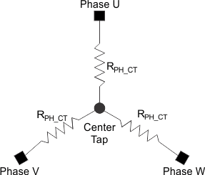
For a wye-connected motor, the motor phase resistance refers to the resistance from the phase output to the center tap, RPH_CT (see Figure 8).
 Figure 8. Wye-Connected Motor Phase Resistance
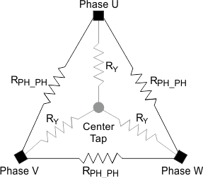
 For a delta-connected motor, the motor phase resistance refers to the equivalent phase to center tap in the wye configuration, which is represented as RY. RPH_CT = RY (see Figure 9).
For both the delta-connected motor and the wye-connected motor, calculating the equivalent RPH_CT is easy by measuring the resistance between two phase terminals (RPH_PH), and then dividing this value by two as shown in Equation 1.
 Figure 9. Delta-Connected Motor and the Equivalent Wye Connections
 The motor phase resistance (RPH_CT) must be converted to a 7-bit digital register value Rm[6:0] to program the motor phase resistance value. The digital register value can be determined as follows:
- Convert the motor phase resistance (RPH_CT) to a digital value where the LSB is weighted to represent 7.35 mΩ: Rmdig = RPH_CT / 0.00735.
- Encode the digital value such that Rmdig = Rm[3:0] << Rm[6:4].
The maximum resistor value, RPH_CT, that can be programmed for the DRV10975 is 14.1 Ω, which represents Rmdig = 1920 and an encoded Rm[6:0] value of 0x7Fh. The minimum resistor the DRV10975 supports is 0.0294 Ω, RPH_CT, which represents Rmdig = 4.
For convenience, the encoded value for Rm[6:0] can also be obtained from Table 2.
Table 2. Motor Phase Resistance Look-Up Table
| RPH_CT (Ω) | RM[6:0] | HEX | RPH_CT (Ω) | RM[6:0] | HEX | RPH_CT (Ω) | RM[6:0] | HEX | ||
|---|---|---|---|---|---|---|---|---|---|---|
| 0 | 000 0000 | 00 | 0.235 | 010 1000 | 28 | 1.88 | 101 1000 | 58 | ||
| 0.0073 | 000 0001 | 01 | 0.264 | 010 1001 | 29 | 2.11 | 101 1001 | 59 | ||
| 0.0147 | 000 0010 | 02 | 0.294 | 010 1010 | 2A | 2.35 | 101 1010 | 5A | ||
| 0.0220 | 000 0011 | 03 | 0.323 | 010 1011 | 2B | 2.58 | 101 1011 | 5B | ||
| 0.0294 | 000 0100 | 04 | 0.352 | 010 1100 | 2C | 2.82 | 101 1100 | 5C | ||
| 0.0367 | 000 0101 | 05 | 0.382 | 010 1101 | 2D | 3.05 | 101 1101 | 5D | ||
| 0.0441 | 000 0110 | 06 | 0.411 | 010 1110 | 2E | 3.29 | 101 1110 | 5E | ||
| 0.0514 | 000 0111 | 07 | 0.441 | 010 1111 | 2F | 3.52 | 101 1111 | 5F | ||
| 0.0588 | 000 1000 | 08 | 0.47 | 011 1000 | 38 | 3.76 | 110 1000 | 68 | ||
| 0.0661 | 000 1001 | 09 | 0.529 | 011 1001 | 39 | 4.23 | 110 1001 | 69 | ||
| 0.0735 | 000 1010 | 0A | 0.588 | 011 1010 | 3A | 4.7 | 110 1010 | 6A | ||
| 0.0808 | 000 1011 | 0B | 0.646 | 011 1011 | 3B | 5.17 | 110 1011 | 6B | ||
| 0.0882 | 000 1100 | 0C | 0.705 | 011 1100 | 3C | 5.64 | 110 1100 | 6C | ||
| 0.0955 | 000 1101 | 0D | 0.764 | 011 1101 | 3D | 6.11 | 110 1101 | 6D | ||
| 0.102 | 000 1110 | 0E | 0.823 | 011 1110 | 3E | 6.58 | 110 1110 | 6E | ||
| 0.110 | 000 1111 | 0F | 0.882 | 011 1111 | 3F | 7.05 | 110 1111 | 6F | ||
| 0.117 | 001 1000 | 18 | 0.94 | 100 1000 | 48 | 7.52 | 111 1000 | 78 | ||
| 0.132 | 001 1001 | 19 | 1.05 | 100 1001 | 49 | 8.46 | 111 1001 | 79 | ||
| 0.147 | 001 1010 | 1A | 1.17 | 100 1010 | 4A | 9.4 | 111 1010 | 7A | ||
| 0.161 | 001 1011 | 1B | 1.29 | 100 1011 | 4B | 10.3 | 111 1011 | 7B | ||
| 0.176 | 001 1100 | 1C | 1.41 | 100 1100 | 4C | 11.2 | 111 1100 | 7C | ||
| 0.191 | 001 1101 | 1D | 1.52 | 100 1101 | 4D | 12.2 | 111 1101 | 7D | ||
| 0.205 | 001 1110 | 1E | 1.64 | 100 1110 | 4E | 13.1 | 111 1110 | 7E | ||
| 0.22 | 001 1111 | 1F | 1.76 | 100 1111 | 4F | 14.1 | 111 1111 | 7F |