JAJSEE9E January   2015  – May 2018 DRV10975

PRODUCTION DATA.  

  1. 特長
  2. アプリケーション
  3. 概要
    1.     アプリケーションの回路図
  4. 改訂履歴
  5. 概要(続き)
  6. Pin Configuration and Functions
    1.     Pin Functions
  7. Specifications
    1. 7.1 Absolute Maximum Ratings
    2. 7.2 ESD Ratings
    3. 7.3 Recommended Operating Conditions
    4. 7.4 Thermal Information
    5. 7.5 Electrical Characteristics
    6. 7.6 Typical Characteristics
  8. Detailed Description
    1. 8.1 Overview
    2. 8.2 Functional Block Diagram
    3. 8.3 Feature Description
      1. 8.3.1 Regulators
        1. 8.3.1.1 Step-Down Regulator
        2. 8.3.1.2 3.3-V and 1.8-V LDO
      2. 8.3.2 Protection Circuits
        1. 8.3.2.1 Thermal Shutdown
        2. 8.3.2.2 Undervoltage Lockout (UVLO)
        3. 8.3.2.3 Overcurrent Protection (OCP)
        4. 8.3.2.4 Lock
      3. 8.3.3 Motor Speed Control
      4. 8.3.4 Sleep or Standby Condition
      5. 8.3.5 Non-Volatile Memory
    4. 8.4 Device Functional Modes
      1. 8.4.1  Motor Parameters
        1. 8.4.1.1 Motor Phase Resistance
        2. 8.4.1.2 BEMF Constant
      2. 8.4.2  Starting the Motor Under Different Initial Conditions
        1. 8.4.2.1 Case 1 – Motor Is Stationary
        2. 8.4.2.2 Case 2 – Motor Is Spinning in the Forward Direction
        3. 8.4.2.3 Case 3 – Motor Is Spinning in the Reverse Direction
      3. 8.4.3  Motor Start Sequence
        1. 8.4.3.1 ISD
        2. 8.4.3.2 Motor Resynchronization
        3. 8.4.3.3 Reverse Drive
        4. 8.4.3.4 Motor Brake
        5. 8.4.3.5 Motor Initialization
          1. 8.4.3.5.1 Align
          2. 8.4.3.5.2 Initial Position Detect (IPD)
            1. 8.4.3.5.2.1 IPD Operation
            2. 8.4.3.5.2.2 IPD Release Mode
            3. 8.4.3.5.2.3 IPD Advance Angle
          3. 8.4.3.5.3 Motor Start
        6. 8.4.3.6 Start-Up Timing
      4. 8.4.4  Start-Up Current Setting
        1. 8.4.4.1 Start-Up Current Ramp-Up
      5. 8.4.5  Closed Loop
        1. 8.4.5.1 Half Cycle Control and Full Cycle Control
        2. 8.4.5.2 Analog Mode Speed Control
        3. 8.4.5.3 Digital PWM Input Mode Speed Control
        4. 8.4.5.4 I2C Mode Speed Control
        5. 8.4.5.5 Closed Loop Accelerate
        6. 8.4.5.6 Control Coefficient
        7. 8.4.5.7 Commutation Control Advance Angle
      6. 8.4.6  Current Limit
        1. 8.4.6.1 Acceleration Current Limit
      7. 8.4.7  Lock Detect and Fault Handling
        1. 8.4.7.1 Lock0: Lock Detection Current Limit Triggered
        2. 8.4.7.2 Lock1: Abnormal Speed
        3. 8.4.7.3 Lock2: Abnormal Kt
        4. 8.4.7.4 Lock3 (Fault3): No Motor Fault
        5. 8.4.7.5 Lock4: Open Loop Motor Stuck Lock
        6. 8.4.7.6 Lock5: Closed Loop Motor Stuck Lock
      8. 8.4.8  AVS Function
        1. 8.4.8.1 Mechanical AVS Function
      9. 8.4.9  PWM Output
      10. 8.4.10 FG Customized Configuration
        1. 8.4.10.1 FG Output Frequency
        2. 8.4.10.2 FG Open-Loop and Lock Behavior
      11. 8.4.11 Diagnostics and Visibility
        1. 8.4.11.1 Motor Status Readback
        2. 8.4.11.2 Motor Speed Readback
          1. 8.4.11.2.1 Two-Byte Register Readback
        3. 8.4.11.3 Motor Electrical Period Readback
        4. 8.4.11.4 BEMF Constant Readback
        5. 8.4.11.5 Motor Estimated Position by IPD
        6. 8.4.11.6 Supply Voltage Readback
        7. 8.4.11.7 Speed Command Readback
        8. 8.4.11.8 Speed Command Buffer Readback
        9. 8.4.11.9 Fault Diagnostics
    5. 8.5 Register Maps
      1. 8.5.1 I2C Serial Interface
      2. 8.5.2 Register Map
      3. 8.5.3 Register Definition
        1. Table 9. Register Description
  9. Application and Implementation
    1. 9.1 Application Information
    2. 9.2 Typical Application
      1. 9.2.1 Design Requirements
      2. 9.2.2 Detailed Design Procedure
      3. 9.2.3 Application Curves
  10. 10Power Supply Recommendations
  11. 11Layout
    1. 11.1 Layout Guidelines
    2. 11.2 Layout Example
  12. 12デバイスおよびドキュメントのサポート
    1. 12.1 デバイス・サポート
      1. 12.1.1 デベロッパー・ネットワークの製品に関する免責事項
    2. 12.2 ドキュメントのサポート
      1. 12.2.1 関連資料
    3. 12.3 商標
    4. 12.4 静電気放電に関する注意事項
    5. 12.5 ドキュメントの更新通知を受け取る方法
    6. 12.6 コミュニティ・リソース
    7. 12.7 Glossary
  13. 13メカニカル、パッケージ、および注文情報

パッケージ・オプション

メカニカル・データ(パッケージ|ピン)
サーマルパッド・メカニカル・データ
発注情報

Mechanical AVS Function

If the speed command suddenly drops such that the BEMF voltage generated by the motor is greater than the voltage that is applied to the motor, then the mechanical energy of the motor is returned to the power supply and the VCC voltage surges. The mechanical AVS function works to prevent this from happening. The DRV10975 buffers the speed command value and limits the resulting output voltage, UMIN, so that it is not less than the BEMF voltage of the motor. The BEMF voltage in the mechanical AVS function is determined using the programmed value for the Kt of the motor (Kt[6:0]) along with the speed. Figure 34 shows the criteria used by the mechanical AVS function.
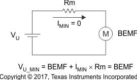
DRV10975 DRV10975Z mech_AVS_LVSCP2.gifFigure 34. Mechanical AVS

The mechanical AVS function can operate in one of two modes, which can be configured by the register bit AVSMMd:

AVSMMd = 0 – AVS mode is always active to prevent the applied voltage from being less than the BEMF voltage.

AVSMMd = 1 – AVS mode becomes active when VCC reaches 24 V. The motor acts as a generator and returns energy into the power supply until VCC reaches 24 V. This mode can be used to enable faster deceleration of the motor in applications where returning energy to the power supply is allowed.