JAJSGG8A november   2018  – august 2020 DRV5057

PRODUCTION DATA  

  1.   1
  2. 特長
  3. アプリケーション
  4. 説明
  5. Revision History
  6. Pin Configuration and Functions
    1.     Pin Functions
  7. Specifications
    1. 6.1 Absolute Maximum Ratings
    2. 6.2 ESD Ratings
    3. 6.3 Recommended Operating Conditions
    4. 6.4 Thermal Information
    5. 6.5 Electrical Characteristics
    6. 6.6 Magnetic Characteristics
    7. 6.7 Typical Characteristics
  8. Detailed Description
    1. 7.1 Overview
    2. 7.2 Functional Block Diagram
    3. 7.3 Feature Description
      1. 7.3.1 Magnetic Flux Direction
      2. 7.3.2 Sensitivity Linearity
      3. 7.3.3 Operating VCC Ranges
      4. 7.3.4 Sensitivity Temperature Compensation for Magnets
      5. 7.3.5 Power-On Time
      6. 7.3.6 Hall Element Location
    4. 7.4 Device Functional Modes
  9. Application and Implementation
    1. 8.1 Application Information
      1. 8.1.1 Selecting the Sensitivity Option
      2. 8.1.2 Decoding a PWM
        1. 8.1.2.1 Decoding a PWM (Digital)
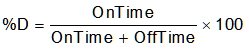
          1. 8.1.2.1.1 Capture and Compare Timer Interrupt
          2. 8.1.2.1.2 Oversampling and Counting With a Timer Interrupt
          3. 8.1.2.1.3 Accuracy and Resolution
        2. 8.1.2.2 Decoding a PWM (Analog)
    2. 8.2 Typical Applications
      1. 8.2.1 Full-Swing Orientation Example
        1. 8.2.1.1 Design Requirements
        2. 8.2.1.2 Detailed Design Procedure
        3. 8.2.1.3 Application Curve
      2. 8.2.2 Half-Swing Orientation Example
        1. 8.2.2.1 Design Requirements
        2. 8.2.2.2 Detailed Design Procedure
    3. 8.3 What to Do and What Not to Do
  10. Power Supply Recommendations
  11. 10Layout
    1. 10.1 Layout Guidelines
    2. 10.2 Layout Examples
  12. 11Device and Documentation Support
    1. 11.1 Documentation Support
      1. 11.1.1 Related Documentation
    2. 11.2 ドキュメントの更新通知を受け取る方法
    3. 11.3 サポート・リソース
    4. 11.4 Trademarks
    5. 11.5 静電気放電に関する注意事項
    6. 11.6 用語集
  13. 12Mechanical, Packaging, and Orderable Information

パッケージ・オプション

メカニカル・データ(パッケージ|ピン)
サーマルパッド・メカニカル・データ
発注情報
Capture and Compare Timer Interrupt

Many microcontrollers have a capture and compare timer mode that can simplify the PWM decoding process. Use the timer in capture and compare mode with an interrupt that triggers on both the rising and falling edges of the signal to obtain both the relative high (on) and low (off) time of the PWM. Make sure that the timer period is significantly faster than the period of the PWM, based on the desired resolution. Calculate the percent duty cycle (%D) of the PWM with Equation 1 by using the relative on and off time of the signal.

Equation 1. GUID-6F1DF86A-0503-4A53-B0E9-A44749094A39-low.gif