JAJSFZ9B October   2017  – January 2021 DRV8873-Q1

PRODUCTION DATA  

  1. 特長
  2. アプリケーション
  3. 概要
  4. Revision History
  5. Pin Configuration and Functions
    1.     Pin Functions
  6. Specifications
    1. 6.1 Absolute Maximum Ratings
    2. 6.2 ESD Ratings
    3. 6.3 Recommended Operating Conditions
    4. 6.4 Thermal Information
    5. 6.5 Electrical Characteristics
    6. 6.6 SPI Timing Requirements
    7. 6.7 Typical Characteristics
  7. Detailed Description
    1. 7.1 Overview
    2. 7.2 Functional Block Diagram
    3. 7.3 Feature Description
      1. 7.3.1 Bridge Control
        1. 7.3.1.1 Control Modes
        2. 7.3.1.2 Half-Bridge Operation
        3. 7.3.1.3 22
        4. 7.3.1.4 Internal Current Sense and Current Regulation
        5. 7.3.1.5 Slew-Rate Control
        6. 7.3.1.6 Dead Time
        7. 7.3.1.7 Propagation Delay
        8. 7.3.1.8 nFAULT Pin
        9. 7.3.1.9 nSLEEP as SDO Reference
      2. 7.3.2 Motor Driver Protection Circuits
        1. 7.3.2.1 VM Undervoltage Lockout (UVLO)
        2. 7.3.2.2 VCP Undervoltage Lockout (CPUV)
        3. 7.3.2.3 Overcurrent Protection (OCP)
          1. 7.3.2.3.1 Latched Shutdown (OCP_MODE = 00b)
          2. 7.3.2.3.2 Automatic Retry (OCP_MODE = 01b)
          3. 7.3.2.3.3 Report Only (OCP_MODE = 10b)
          4. 7.3.2.3.4 Disabled (OCP_MODE = 11b)
        4. 7.3.2.4 Open-Load Detection (OLD)
          1. 7.3.2.4.1 Open-Load Detection in Passive Mode (OLP)
          2. 7.3.2.4.2 Open-Load Detection in Active Mode (OLA)
        5. 7.3.2.5 Thermal Shutdown (TSD)
          1. 7.3.2.5.1 Latched Shutdown (TSD_MODE = 0b)
          2. 7.3.2.5.2 Automatic Recovery (TSD_MODE = 1b)
        6. 7.3.2.6 Thermal Warning (OTW)
      3. 7.3.3 Hardware Interface
        1. 7.3.3.1 MODE (Tri-Level Input)
        2. 7.3.3.2 Slew Rate
    4. 7.4 Device Functional Modes
      1. 7.4.1 Motor Driver Functional Modes
        1. 7.4.1.1 Sleep Mode (nSLEEP = 0)
        2. 7.4.1.2 Disable Mode (nSLEEP = 1, DISABLE = 1)
        3. 7.4.1.3 Operating Mode (nSLEEP = 1, DISABLE = 0)
        4. 7.4.1.4 nSLEEP Reset Pulse
    5. 7.5 Programming
      1. 7.5.1 Serial Peripheral Interface (SPI) Communication
        1. 7.5.1.1 SPI Format
        2. 7.5.1.2 SPI for a Single Slave Device
        3. 7.5.1.3 SPI for Multiple Slave Devices in Parallel Configuration
        4. 7.5.1.4 SPI for Multiple Slave Devices in Daisy Chain Configuration
    6. 7.6 Register Maps
  8. Application and Implementation
    1. 8.1 Application Information
    2. 8.2 Typical Application
      1. 8.2.1 Design Requirements
        1. 8.2.1.1 Motor Voltage
        2. 8.2.1.2 Drive Current and Power Dissipation
        3. 8.2.1.3 Sense Resistor
      2. 8.2.2 Detailed Design Procedure
        1. 8.2.2.1 Thermal Considerations
        2. 8.2.2.2 Heatsinking
      3. 8.2.3 Application Curves
  9. Power Supply Recommendations
    1. 9.1 Bulk Capacitance Sizing
  10. 10Layout
    1. 10.1 Layout Guidelines
    2. 10.2 Layout Example
  11. 11Device and Documentation Support
    1. 11.1 Documentation Support
      1. 11.1.1 Related Documentation
    2. 11.2 Receiving Notification of Documentation Updates
    3. 11.3 サポート・リソース
    4. 11.4 Trademarks
    5. 11.5 静電気放電に関する注意事項
    6. 11.6 用語集
  12. 12Mechanical, Packaging, and Orderable Information

パッケージ・オプション

メカニカル・データ(パッケージ|ピン)
サーマルパッド・メカニカル・データ
発注情報

nFAULT Pin

The nFAULT pin has an open-drain output and should be pulled up to a 5-V or 3.3-V supply. When a fault is detected, the nFAULT line is logic low. For a 5-V pullup the nFAULT pin can be tied to the DVDD pin with a resistor (see the Section 8 section). For a 3.3-V pullup, an external 3.3-V supply must be used.
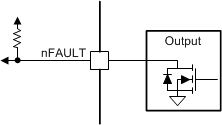
GUID-B4062AA4-BB0B-4EAF-8FA0-49358D4BD81E-low.gifFigure 7-10 nFAULT Pin

During the device power-up sequence, or when exiting sleep mode, the nFAULT pin is held low until the digital core is alive and functional. This low level signal on the nFAULT line does not represent a fault condition. The signal can be used by the external MCU to determine when the digital core of the device is ready; however, this does not mean that the device is ready to accept input commands via the INx pins.