JAJSGV8B September 2019 – December 2019 DRV8904-Q1 , DRV8906-Q1 , DRV8908-Q1 , DRV8910-Q1 , DRV8912-Q1
UNLESS OTHERWISE NOTED, this document contains PRODUCTION DATA.
- 1 特長
- 2 アプリケーション
- 3 概要
- 4 改訂履歴
- 5 Device Comparison Table
- 6 Pin Configuration and Functions
- 7 Specifications
-
8 Detailed Description
- 8.1 Overview
- 8.2 Functional Block Diagram
- 8.3
Feature Description
- 8.3.1
Half Bridge Drivers
- 8.3.1.1
Control Modes
- 8.3.1.1.1 Continuous Mode (Without PWM)
- 8.3.1.1.2 Chopping Mode (With PWM)
- 8.3.1.1.3 Parallel Mode (Continuous Operation)
- 8.3.1.1.4
Parallel Mode (PWM Operation)
- 8.3.1.1.4.1 PWM Configuration
- 8.3.1.1.4.2 Free-Wheeling Mode (Synchronous Rectification) Disable / Enable
- 8.3.1.1.4.3 PWM Channels Mapping
- 8.3.1.1.4.4 PWM Channels Configuration (PWM Frequency and PWM Duty)
- 8.3.1.1.4.5 PWM Generators Disable
- 8.3.1.1.4.6 Half-Bridge Enable
- 8.3.1.1.4.7 PWM Generators Enable
- 8.3.1.2 Half-Bridge Drive Architecture
- 8.3.1.1
Control Modes
- 8.3.2 Pin Diagrams
- 8.3.3 Protection Circuits
- 8.3.1
Half Bridge Drivers
- 8.4 Device Functional Modes
- 8.5 Programming
- 8.6
Register Map
- 8.6.1
DRV8912-Q1 and DRV8910-Q1 Register Maps
- 8.6.1.1
Status Registers
- 8.6.1.1.1 IC Status (IC_STAT) Register (Address = 0x00) [reset = 0x00]
- 8.6.1.1.2 Overcurrent Protection (OCP) Status 1 (OCP_STAT_1) Register (Address = 0x01) [reset = 0x00]
- 8.6.1.1.3 Overcurrent Protection (OCP) Status 2 (OCP_STAT_2) Register (Address = 0x02) [reset = 0x00]
- 8.6.1.1.4 Overcurrent Protection (OCP) Status 3 (OCP_STAT_3) Register (Address = 0x03) [reset = 0x00]
- 8.6.1.1.5 Open-Load Detect (OLD) Status 1 (OLD_STAT_1) Register (Address = 0x04) [reset = 0x00]
- 8.6.1.1.6 Open-Load Detect (OLD) Status 2 (OLD_STAT_2) Register (Address = 0x05) [reset = 0x00]
- 8.6.1.1.7 Open-Load Detect (OLD) Status 3 (OLD_STAT_3) Register (Address = 0x06) [reset = 0x00]
- 8.6.1.2
Control Registers
- 8.6.1.2.1 Configuration (CONFIG_CTRL) Register (Address = 0x07) [reset = 0x00]
- 8.6.1.2.2 Operation Control 1 (OP_CTRL_1) Register (Address = 0x08) [reset = 0x00]
- 8.6.1.2.3 Operation Control 2 (OP_CTRL_2) Register (Address = 0x09) [reset = 0x00]
- 8.6.1.2.4 Operation Control 3 (OP_CTRL_3) Register (Address = 0x0A) [reset = 0x00]
- 8.6.1.2.5 PWM Control 1 (PWM_CTRL_1) Register (Address = 0x0B) [reset = 0x00]
- 8.6.1.2.6 PWM Control 2 (PWM_CTRL_2) Register (Address = 0x0C) [reset = 0x00]
- 8.6.1.2.7 Free-Wheeling Control 1 (FW_CTRL_1) Register (Address = 0x0D) [reset = 0x00]
- 8.6.1.2.8 Free-Wheeling Control 2 (FW_CTRL_2) Register (Address = 0x0E) [reset = 0x00]
- 8.6.1.2.9 PWM Map Control 1 (PWM_MAP_CTRL_1) Register (Address = 0x0F) [reset = 0x00]
- 8.6.1.2.10 PWM Map Control 2 (PWM_MAP_CTRL_2) Register (Address = 0x10) [reset = 0x00]
- 8.6.1.2.11 PWM Map Control 3 (PWM_MAP_CTRL_3) Register (Address = 0x11) [reset = 0x00]
- 8.6.1.2.12 PWM Frequency Control (PWM_FREQ_CTRL) Register (Address = 0x12) [reset = 0x00]
- 8.6.1.2.13 PWM Duty Control Channel 1 (PWM_DUTY_CH1) Register (Address = 0x13) [reset = 0x00]
- 8.6.1.2.14 PWM Duty Control Channel 2 (PWM_DUTY_CH2) Register (Address = 0x14) [reset = 0x00]
- 8.6.1.2.15 PWM Duty Control Channel 3 (PWM_DUTY_CH3) Register (Address = 0x15) [reset = 0x00]
- 8.6.1.2.16 PWM Duty Control Channel 4 (PWM_DUTY_CH4) Register (Address = 0x16) [reset = 0x00]
- 8.6.1.2.17 Slew Rate Control 1 (SR_CTRL_1) Register (Address = 0x17) [reset = 0x00]
- 8.6.1.2.18 Slew Rate Control 2 (SR_CTRL_2) Register (Address = 0x18) [reset = 0x00]
- 8.6.1.2.19 Open-Load Detect (OLD) Control 1 (OLD_CTRL_1) Register (Address = 0x19) [reset = 0x00]
- 8.6.1.2.20 Open-Load Detect (OLD) Control 2 (OLD_CTRL_2) Register (Address = 0x1A) [reset = 0x00]
- 8.6.1.2.21 Open-Load Detect (OLD) Control 3 (OLD_CTRL_3) Register (Address = 0x1B) [reset = 0x00]
- 8.6.1.2.22 Open-Load Detect (OLD) Control 4 (OLD_CTRL_4) Register (Address = 0x24) [reset = 0x00]
- 8.6.1.1
Status Registers
- 8.6.2
DRV8908-Q1, DRV8906-Q1 and DRV8904-Q1 Register Maps
- 8.6.2.1
Status Registers
- 8.6.2.1.1 IC Status (IC_STAT) Register (Address = 0x00) [reset = 0x00]
- 8.6.2.1.2 Overcurrent Protection (OCP) Status 1 (OCP_STAT_1) Register (Address = 0x01) [reset = 0x00]
- 8.6.2.1.3 Overcurrent Protection (OCP) Status 2 (OCP_STAT_2) Register (Address = 0x02) [reset = 0x00]
- 8.6.2.1.4 Overcurrent Protection (OCP) Status 3 (OCP_STAT_3) Register (Address = 0x03) [reset = 0x00]
- 8.6.2.1.5 Open-Load Detect (OLD) Status 1 (OLD_STAT_1) Register (Address = 0x04) [reset = 0x00]
- 8.6.2.1.6 Open-Load Detect (OLD) Status 2 (OLD_STAT_2) Register (Address = 0x05) [reset = 0x00]
- 8.6.2.1.7 Open-Load Detect (OLD) Status 3 (OLD_STAT_3) Register (Address = 0x06) [reset = 0x00]
- 8.6.2.2
Control Registers
- 8.6.2.2.1 Configuration (CONFIG_CTRL) Register (Address = 0x07) [reset = 0x00]
- 8.6.2.2.2 Operation Control 1 (OP_CTRL_1) Register (Address = 0x08) [reset = 0x00]
- 8.6.2.2.3 Operation Control 2 (OP_CTRL_2) Register (Address = 0x09) [reset = 0x00]
- 8.6.2.2.4 Operation Control 3 (OP_CTRL_3) Register (Address = 0x0A) [reset = 0x00]
- 8.6.2.2.5 PWM Control 1 (PWM_CTRL_1) Register (Address = 0x0B) [reset = 0x00]
- 8.6.2.2.6 PWM Control 2 (PWM_CTRL_2) Register (Address = 0x0C) [reset = 0x00]
- 8.6.2.2.7 Free-Wheeling Control 1 (FW_CTRL_1) Register (Address = 0x0D) [reset = 0x00]
- 8.6.2.2.8 Free-Wheeling Control 2 (FW_CTRL_2) Register (Address = 0x0E) [reset = 0x00]
- 8.6.2.2.9 PWM Map Control 1 (PWM_MAP_CTRL_1) Register (Address = 0x0F) [reset = 0x00]
- 8.6.2.2.10 PWM Map Control 2 (PWM_MAP_CTRL_2) Register (Address = 0x10) [reset = 0x00]
- 8.6.2.2.11 PWM Map Control 3 (PWM_MAP_CTRL_3) Register (Address = 0x11) [reset = 0x00]
- 8.6.2.2.12 PWM Map Control 4 (PWM_MAP_CTRL_4) Register (Address = 0x12) [reset = 0x00]
- 8.6.2.2.13 PWM Frequency Control 1 (PWM_FREQ_CTRL_1) Register (Address = 0x13 [reset = 0x00]
- 8.6.2.2.14 PWM Frequency Control 2 (PWM_FREQ_CTRL_2) Register (Address = 0x14 [reset = 0x00]
- 8.6.2.2.15 PWM Duty Control Channel 1 (PWM_DUTY_CH1) Register (Address = 0x15) [reset = 0x00]
- 8.6.2.2.16 PWM Duty Control Channel 2 (PWM_DUTY_CH2) Register (Address = 0x16) [reset = 0x00]
- 8.6.2.2.17 PWM Duty Control Channel 3 (PWM_DUTY_CH3) Register (Address = 0x17) [reset = 0x00]
- 8.6.2.2.18 PWM Duty Control Channel 4 (PWM_DUTY_CH4) Register (Address = 0x18) [reset = 0x00]
- 8.6.2.2.19 PWM Duty Control Channel 5 (PWM_DUTY_CH5) Register (Address = 0x19) [reset = 0x00]
- 8.6.2.2.20 PWM Duty Control Channel 6 (PWM_DUTY_CH6) Register (Address = 0x1A) [reset = 0x00]
- 8.6.2.2.21 PWM Duty Control Channel 7 (PWM_DUTY_CH7) Register (Address = 0x1B) [reset = 0x00]
- 8.6.2.2.22 PWM Duty Control Channel 8 (PWM_DUTY_CH8) Register (Address = 0x1C) [reset = 0x00]
- 8.6.2.2.23 Slew Rate Control 1 (SR_CTRL_1) Register (Address = 0x1D [reset = 0x00]
- 8.6.2.2.24 Slew Rate Control 2 (SR_CTRL_2) Register (Address = 0x1E) [reset = 0x00]
- 8.6.2.2.25 Open-Load Detect (OLD) Control 1 (OLD_CTRL_1) Register (Address = 0x1F) [reset = 0x00]
- 8.6.2.2.26 Open-Load Detect (OLD) Control 2 (OLD_CTRL_2) Register (Address = 0x20) [reset = 0x00]
- 8.6.2.2.27 Open-Load Detect (OLD) Control 3 (OLD_CTRL_3) Register (Address = 0x21) [reset = 0x00]
- 8.6.2.2.28 Open Load Detect (OLD) Control 4 (OLD_CTRL_4) Register (Address = 0x22) [reset = 0x00]
- 8.6.2.2.29 Open Load Detect (OLD) Control 5 (OLD_CTRL_5) Register (Address = 0x23) [reset = 0x00]
- 8.6.2.2.30 Open Load Detect (OLD) Control 6 (OLD_CTRL_6) Register (Address = 0x24) [reset = 0x00]
- 8.6.2.1
Status Registers
- 8.6.1
DRV8912-Q1 and DRV8910-Q1 Register Maps
- 9 Application and Implementation
- 10Power Supply Recommendations
- 11Layout
- 12デバイスおよびドキュメントのサポート
- 13メカニカル、パッケージ、および注文情報
パッケージ・オプション
メカニカル・データ(パッケージ|ピン)
- PWP|24
サーマルパッド・メカニカル・データ
- PWP|24
発注情報
8.5.3.1 SPI Interface for Multiple Slaves in Daisy Chain
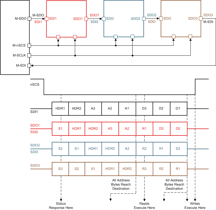
The DRV89XX-Q1 device can be connected in a daisy chain configuration to save GPIO ports when multiple devices are communicating to the same MCU. Figure 64 shows the topology when 3 devices are connected in series with waveforms.
 Figure 64. Daisy Chain SPI Operation
 The first device in the chain shown above receives data from the master controller in the following format. See SDI1 in Figure 64
- 2 bytes of Header
- 3 bytes of Address
- 3 bytes of Data
After the data has been transmitted through the chain, the master controller receives it in the following format. See SDO3 in Figure 64
- 3 bytes of Status
- 2 bytes of Header (should be identical to the information controller sent)
- 3 bytes of Report
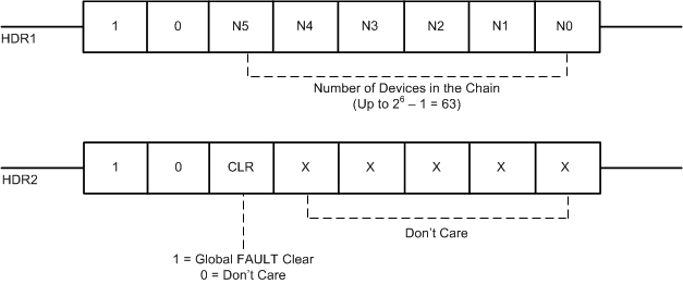
The Header bytes contain information of the number of devices connected in the chain, and a global clear fault command that will clear the fault registers of all the devices on the rising edge of the chip select (nSCS) signal. N5 through N0 are 6 bits dedicated to show the number of devices in the chain as shown in Figure 65. Up to 63 devices can be connected in series per daisy chain connection.
The 5 LSBs of the HDR2 register are don’t care bits that can be used by the MCU to determine integrity of the daisy chain connection. Header bytes must start with 1 and 0 for the two MSBs.
 Figure 65. Header Bits
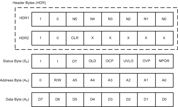
 The Status byte provides information about the fault status register for each device in the daisy chain as shown in Figure 66. That way the master controller does not have to initiate a read command to read the fault status from any particular device. This saves the controller additional read commands and makes the system more efficient to determine fault conditions flagged in a device.
 Figure 66. Daisy Chain Read Registers
 When data passes through a device, it determines the position of itself in the chain by counting the number of Status bytes it receives following by the first Header byte. For example, in this 3 device configuration, device 2 in the chain will receive two Status bytes before receiving HDR1 byte, followed by HDR2 byte.
From the two Status bytes it knows that its position is second in the chain, and from HDR2 byte it knows how many devices are connected in the chain. That way it only loads the relevant address and data byte in its buffer and bypasses the other bits. This protocol allows for faster communication without adding latency to the system for up to 63 devices in the chain.
The address and data bytes remain the same with respect to a single device connection. The Report bytes (R1 through R3), as shown in the figure above, is the content of the register being accessed.
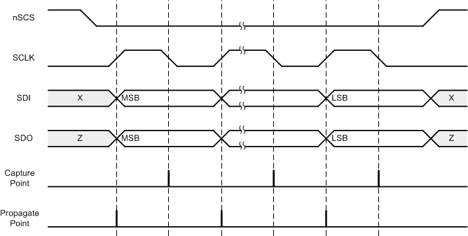
 Figure 67. SPI Slave Timing Diagram