JAJSI57B September 2016 – February 2024 DS280DF810
PRODUCTION DATA
- 1
- 1 特長
- 2 アプリケーション
- 3 概要
- 4 Pin Configuration and Functions
-
5 Specifications
- 5.1 Absolute Maximum Ratings
- 5.2 ESD Ratings
- 5.3 Recommended Operating Conditions
- 5.4 Thermal Information
- 5.5 Electrical Characteristics
- 5.6 Timing Requirements, Retimer Jitter Specifications
- 5.7 Timing Requirements, Retimer Specifications
- 5.8 Timing Requirements, Recommended Calibration Clock Specifications
- 5.9 Recommended SMBus Switching Characteristics (Target Mode)
- 5.10 Recommended SMBus Switching Characteristics (Controller Mode)
- 5.11 Typical Characteristics
-
6 Detailed Description
- 6.1 Overview
- 6.2 Functional Block Diagram
- 6.3
Feature Description
- 6.3.1
Device Data Path Operation
- 6.3.1.1 AC-Coupled Receiver and Transmitter
- 6.3.1.2 Signal Detect
- 6.3.1.3 Continuous Time Linear Equalizer (CTLE)
- 6.3.1.4 Variable Gain Amplifier (VGA)
- 6.3.1.5 2x2 Cross-Point Switch
- 6.3.1.6 Decision Feedback Equalizer (DFE)
- 6.3.1.7 Clock and Data Recovery (CDR)
- 6.3.1.8 Calibration Clock
- 6.3.1.9 Differential Driver with FIR Filter
- 6.3.2 Debug Features
- 6.3.1
Device Data Path Operation
- 6.4 Device Functional Modes
- 6.5 Programming
- 6.6 Register Maps
- 7 Application and Implementation
- 8 Device and Documentation Support
- 9 Revision History
- 10Mechanical, Packaging, and Orderable Information
パッケージ・オプション
デバイスごとのパッケージ図は、PDF版データシートをご参照ください。
メカニカル・データ(パッケージ|ピン)
- ABW|135
- ABV|135
サーマルパッド・メカニカル・データ
発注情報
7.2.2 Front-Port Jitter Cleaning Application
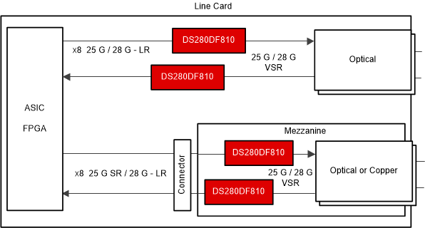
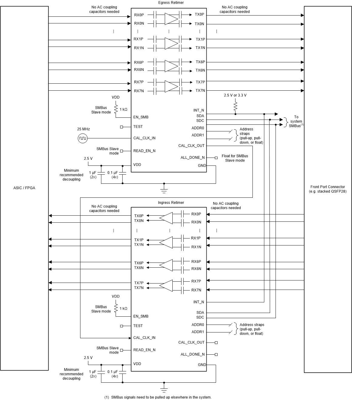
The DS280DF810 has strong equalization capabilities that allow it to equalize insertion loss, reduce jitter, and extend the reach of front-port interfaces. A single DS280DF810 can be used to support all eight egress channels for a stacked QSFP cage. Another DS280DF810 can be used to support all eight ingress channels for the same stacked QSFP cage. Alternatively, a single DS280DF810 can be used to support all egress and ingress channels for a single QSFP port.
For applications which require IEEE802.3 100GBASE-CR4 or 25GBASE-CR auto-negotiation and link training, a linear repeater device such as the DS280BR820 (or similar) is recommended.
Figure 7-4 illustrates this configuration, and Section 5.6 shows an example simplified schematic for a typical front-port application.
 Figure 7-4 Front-Port Application Block Diagram
 Figure 7-5 Front-Port Application Schematic