JAJSAG9M November 2005 – January 2017 DS90C124 , DS90C241
PRODUCTION DATA.
- 1 特長
- 2 アプリケーション
- 3 概要
- 4 改訂履歴
- 5 概要(続き)
- 6 Pin Configuration and Functions
- 7 Specifications
- 8 Parameter Measurement Information
- 9 Detailed Description
- 10Applications and Implementation
- 11Power Supply Recommendations
- 12Layout
- 13デバイスおよびドキュメントのサポート
- 14メカニカル、パッケージ、および注文情報
パッケージ・オプション
メカニカル・データ(パッケージ|ピン)
- PFB|48
サーマルパッド・メカニカル・データ
- PFB|48
発注情報
8 Parameter Measurement Information
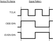 Figure 3. Serializer Input Checkerboard Pattern
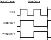 Figure 4. Deserializer Output Checkerboard Pattern
 Figure 5. Serializer LVDS Output Load and Transition Times
 Figure 6. Serializer Input Clock Transition Times
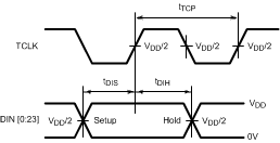 Figure 7. Serializer Setup and Hold Times
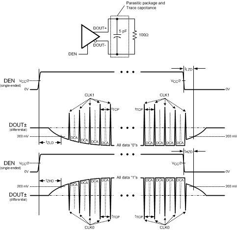 Figure 8. Serializer TRI-STATE Test Circuit and Delay
 Figure 9. Serializer PLL Lock Time and TPWDNB TRI-STATE Delays
 Figure 10. Serializer Delay
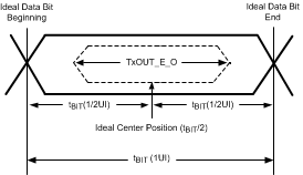 Figure 11. Transmitter Output Eye Opening (TxOUT_E_O)
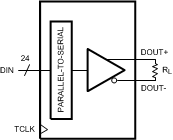
VOD = (DOUT+) – (DOUT -)
Differential output signal is shown as (DOUT+) – (DOUT -) with the device in data transfer mode.
Figure 12. Serializer VOD Diagram
Differential output signal is shown as (DOUT+) – (DOUT -) with the device in data transfer mode.
 Figure 13. Deserializer LVCMOS/LVTTL Output Load and Transition Times
 Figure 14. Deserializer Delay
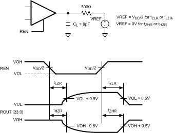
CL includes instrumentation and fixture capacitance within 6 cm of ROUT[23:0].
Figure 15. Deserializer TRI-STATE Test Circuit and Timing
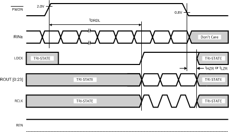 Figure 16. Deserializer PLL Lock Times and RPWDNB TRI-STATE Delay
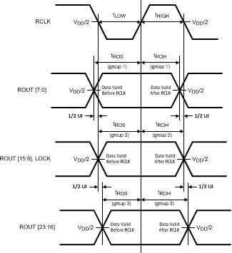 Figure 17. Deserializer Setup and Hold Times
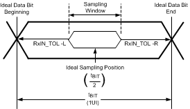
RxIN_TOL_L is the ideal noise margin on the left of the figure with respect to ideal.
RxIN_TOL_R is the ideal noise margin on the right of the figure with respect to ideal.
Figure 18. Receiver Input Tolerance (RxIN_TOL) and Sampling Window
RxIN_TOL_R is the ideal noise margin on the right of the figure with respect to ideal.