JAJSH49B march 2019 – march 2023 DS90UB953A-Q1
PRODUCTION DATA
- 1 特長
- 2 アプリケーション
- 3 概要
- 4 Revision History
- 5 Pin Configuration and Functions
- 6 Specifications
-
7 Detailed Description
- 7.1 Overview
- 7.2 Functional Block Diagram
- 7.3
Feature Description
- 7.3.1 CSI-2 Receiver
- 7.3.2 FPD-Link III Forward Channel Transmitter
- 7.3.3 FPD-Link III Back Channel Receiver
- 7.3.4 Serializer Status and Monitoring
- 7.3.5 FrameSync Operation
- 7.3.6 GPIO Support
- 7.4 Device Functional Modes
- 7.5 Programming
- 7.6 Pattern Generation
- 7.7
Register Maps
- 7.7.1 I2C Device ID Register
- 7.7.2 Reset
- 7.7.3 General Configuration
- 7.7.4 Forward Channel Mode Selection
- 7.7.5 BC_MODE_SELECT
- 7.7.6 PLL Clock Control
- 7.7.7 Clock Output Control 0
- 7.7.8 Clock Output Control 1
- 7.7.9 Back Channel Watchdog Control
- 7.7.10 I2C Control 1
- 7.7.11 I2C Control 2
- 7.7.12 SCL High Time
- 7.7.13 SCL Low Time
- 7.7.14 Local GPIO DATA
- 7.7.15 GPIO Input Control
- 7.7.16 RESERVED Register
- 7.7.17 DVP_CFG
- 7.7.18 DVP_DT
- 7.7.19 RESERVED Register
- 7.7.20 Force BIST Error
- 7.7.21 Remote BIST Control
- 7.7.22 Sensor Voltage Gain
- 7.7.23 RESERVED Register
- 7.7.24 Sensor Control 0
- 7.7.25 Sensor Control 1
- 7.7.26 Voltage Sensor 0 Thresholds
- 7.7.27 Voltage Sensor 1 Thresholds
- 7.7.28 Temperature Sensor Thresholds
- 7.7.29 CSI-2 Alarm Enable
- 7.7.30 Alarm Sense Enable
- 7.7.31 Back Channel Alarm Enable
- 7.7.32 RESERVED Register
- 7.7.33 CSI-2 Polarity Select
- 7.7.34 CSI-2 LP Mode Polarity
- 7.7.35 CSI-2 High-Speed RX Enable
- 7.7.36 CSI-2 Low Power Enable
- 7.7.37 CSI-2 Termination Enable
- 7.7.38 RESERVED Register
- 7.7.39 RESERVED Register
- 7.7.40 RESERVED Register
- 7.7.41 RESERVED Register
- 7.7.42 RESERVED Register
- 7.7.43 RESERVED Register
- 7.7.44 RESERVED Register
- 7.7.45 RESERVED Register
- 7.7.46 CSI-2 Packet Header Control
- 7.7.47 Back Channel Configuration
- 7.7.48 Datapath Control 1
- 7.7.49 RESERVED Register
- 7.7.50 Remote Partner Capabilities 1
- 7.7.51 RESERVED Register
- 7.7.52 Partner Deserializer ID
- 7.7.53 RESERVED Register
- 7.7.54 Target 0 ID
- 7.7.55 Target 1 ID
- 7.7.56 Target 2 ID
- 7.7.57 Target 3 ID
- 7.7.58 Target 4 ID
- 7.7.59 Target 5 ID
- 7.7.60 Target 6 ID
- 7.7.61 Target 7 ID
- 7.7.62 Target 0 Alias
- 7.7.63 Target 1 Alias
- 7.7.64 Target 2 Alias
- 7.7.65 Target 3 Alias
- 7.7.66 Target 4 Alias
- 7.7.67 Target 5 Alias
- 7.7.68 Target 6 Alias
- 7.7.69 Target 7 Alias
- 7.7.70 Back Channel Control
- 7.7.71 Revision ID
- 7.7.72 Device Status
- 7.7.73 General Status
- 7.7.74 GPIO Pin Status
- 7.7.75 BIST Error Count
- 7.7.76 CRC Error Count 1
- 7.7.77 CRC Error Count 2
- 7.7.78 Sensor Status
- 7.7.79 Sensor V0
- 7.7.80 Sensor V1
- 7.7.81 Sensor T
- 7.7.82 RESERVED Register
- 7.7.83 CSI-2 Error Count
- 7.7.84 CSI-2 Error Status
- 7.7.85 CSI-2 Errors Data Lanes 0 and 1
- 7.7.86 CSI-2 Errors Data Lanes 2 and 3
- 7.7.87 CSI-2 Errors Clock Lane
- 7.7.88 CSI-2 Packet Header Data
- 7.7.89 Packet Header Word Count 0
- 7.7.90 Packet Header Word Count 1
- 7.7.91 CSI-2 ECC
- 7.7.92 RESERVED Register
- 7.7.93 RESERVED Register
- 7.7.94 RESERVED Register
- 7.7.95 RESERVED Register
- 7.7.96 RESERVED Register
- 7.7.97 RESERVED Register
- 7.7.98 RESERVED Register
- 7.7.99 RESERVED Register
- 7.7.100 RESERVED Register
- 7.7.101 RESERVED Register
- 7.7.102 RESERVED Register
- 7.7.103 RESERVED Register
- 7.7.104 RESERVED Register
- 7.7.105 RESERVED Register
- 7.7.106 RESERVED Register
- 7.7.107 RESERVED Register
- 7.7.108 RESERVED Register
- 7.7.109 RESERVED Register
- 7.7.110 RESERVED Register
- 7.7.111 RESERVED Register
- 7.7.112 RESERVED Register
- 7.7.113 RESERVED Register
- 7.7.114 RESERVED Register
- 7.7.115 RESERVED Register
- 7.7.116 RESERVED Register
- 7.7.117 RESERVED Register
- 7.7.118 RESERVED Register
- 7.7.119 RESERVED Register
- 7.7.120 RESERVED Register
- 7.7.121 RESERVED Register
- 7.7.122 RESERVED Register
- 7.7.123 IND_ACC_CTL
- 7.7.124 IND_ACC_ADDR
- 7.7.125 IND_ACC_DATA
- 7.7.126 RESERVED Register
- 7.7.127 FPD3_TX_ID0
- 7.7.128 FPD3_TX_ID1
- 7.7.129 FPD3_TX_ID2
- 7.7.130 FPD3_TX_ID3
- 7.7.131 FPD3_TX_ID4
- 7.7.132 FPD3_TX_ID5
- 7.7.133
Indirect Access Registers
- 7.7.133.1 Reserved
- 7.7.133.2 PGEN_CTL
- 7.7.133.3 PGEN_CFG
- 7.7.133.4 PGEN_CSI_DI
- 7.7.133.5 PGEN_LINE_SIZE1
- 7.7.133.6 PGEN_LINE_SIZE0
- 7.7.133.7 PGEN_BAR_SIZE1
- 7.7.133.8 PGEN_BAR_SIZE0
- 7.7.133.9 PGEN_ACT_LPF1
- 7.7.133.10 PGEN_ACT_LPF0
- 7.7.133.11 PGEN_TOT_LPF1
- 7.7.133.12 PGEN_TOT_LPF0
- 7.7.133.13 PGEN_LINE_PD1
- 7.7.133.14 PGEN_LINE_PD0
- 7.7.133.15 PGEN_VBP
- 7.7.133.16 PGEN_VFP
- 7.7.133.17 PGEN_COLOR0
- 7.7.133.18 PGEN_COLOR1
- 7.7.133.19 PGEN_COLOR2
- 7.7.133.20 PGEN_COLOR3
- 7.7.133.21 PGEN_COLOR4
- 7.7.133.22 PGEN_COLOR5
- 7.7.133.23 PGEN_COLOR6
- 7.7.133.24 PGEN_COLOR7
- 7.7.133.25 PGEN_COLOR8
- 7.7.133.26 PGEN_COLOR9
- 7.7.133.27 PGEN_COLOR10
- 7.7.133.28 PGEN_COLOR11
- 7.7.133.29 PGEN_COLOR12
- 7.7.133.30 PGEN_COLOR13
- 7.7.133.31 PGEN_COLOR14
- 7.7.133.32 PGEN_COLOR15
- 8 Application and Implementation
- 9 Power Supply Recommendations
- 10Layout
- 11Device and Documentation Support
- 12Mechanical, Packaging, and Orderable Information
パッケージ・オプション
メカニカル・データ(パッケージ|ピン)
- RHB|32
サーマルパッド・メカニカル・データ
- RHB|32
発注情報
8.1.1 Power-over-Coax
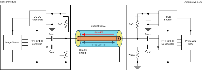
The DS90UB953A-Q1 is designed to support the Power-over-Coax (PoC) method of powering remote sensor systems. With this method, the power is delivered over the same medium (a coaxial cable) used for high-speed digital video data, bidirectional control, and diagnostics data transmission. This method uses passive networks or filters that isolate the transmission line from the loading of the DC-DC regulator circuits and their connecting power traces on both sides of the link as shown in Figure 8-1.
 Figure 8-1 Power-over-Coax (PoC) System Diagram
The PoC networks' impedance of ≥ 1 kΩ over a specific frequency band is recommended to isolate the transmission line from the loading of the regulator circuits. Higher PoC network impedance will contribute to favorable insertion loss and return loss characteristics in the high-speed channel. The lower limit of the frequency band is defined as ½ of the frequency of the back channel, fBC. The upper limit of the frequency band is the frequency of the forward high-speed channel, fFC. However, the main criteria that need to be met in the total high-speed channel, which consists of a serializer PCB, a deserializer PCB, and a cable, are the insertion loss and return loss limits defined in the Total Channel Requirements(1) over the entire system, while the system is under maximum current load and extreme temperature conditions (2).
|
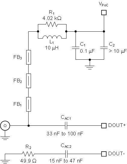
 Figure 8-2 Typical PoC Network for a "4G" FPD-Link III
Table 8-1 lists essential components for this particular PoC network. Note that the impedance characteristic of the ferrite beads deviates with the bias current. Therefore, keeping the current going through the network below 150 mA is recommended.
| COUNT | REF DES | DESCRIPTION | PART NUMBER | MFR |
|---|---|---|---|---|
| 1 | L1 | Inductor, 10 µH, 0.288 Ω maximum, 530 mA minimum (Isat, Itemp) 30 MHz SRF minimum, 3 mm × 3 mm, General-Purpose | LQH3NPN100MJR | Murata |
| Inductor, 10 µH, 0.288 Ω maximum, 530 mA minimum (Isat, Itemp) 30 MHz SRF minimum, 3 mm × 3 mm, AEC-Q200 | LQH3NPZ100MJR | Murata | ||
| Inductor, 10 µH, 0.360 Ω maximum, 450 mA minimum (Isat, Itemp) 30 MHz SRF minimum, 3.2 mm × 2.5 mm, AEC-Q200 | NLCV32T-100K-EFD | TDK | ||
| Inductor, 10 µH, 0.400 Ω typical, 550 mA minimum (Isat, Itemp) 39 MHz SRF typical, 3 mm × 3 mm, AEC-Q200 | TYS3010100M-10 | Laird | ||
| Inductor, 10 µH, 0.325 Ω maximum, 725 mA minimum (Isat, Itemp) 41 MHz SRF typical, 3 mm × 3 mm, AEC-Q200 | TYS3015100M-10 | Laird | ||
| 3 | FB1-FB3 | Ferrite Bead, 1.5 kΩ at 1 GHz, 0.5 Ω maximum at DC 500 mA at 85°C, 0603 SMD , General-Purpose | BLM18HE152SN1 | Murata |
| Ferrite Bead, 1.5 kΩ at 1 GHz, 0.5 Ω maximum at DC 500 mA at 85°C, 0603 SMD , AEC-Q200 | BLM18HE152SZ1 | Murata |
In addition to the selection of PoC network components, their placement and layout play a critical role as well.
- Place the smallest component, typically a ferrite bead or a chip inductor, as close to the connector as possible. Route the high-speed trace through one of its pads to avoid stubs.
- Use the smallest component pads as allowed by manufacturer's design rules. Add anti-pads in the inner planes below the component pads to minimize impedance drop.
- Consult with the connector manufacturer for optimized connector footprint. If the connector is mounted on the same side as the IC, minimize the impact of the through-hole connector stubs by routing the high-speed signal traces on the opposite side of the connector mounting side.
- Use coupled 100-Ω differential signal traces from the device pins to the AC-coupling caps. Use 50-Ω single-ended traces from the AC-coupling capacitors to the connector.
- Terminate the inverting signal traces close to the connectors with standard 49.9-Ω resistors.
The suggested characteristics for single-ended PCB traces (microstrips or striplines) for serializer or deserializer boards are listed in Table 8-2. The effects of the PoC networks must be accounted for when testing the traces for compliance to the suggested limits.
| PARAMETER | MIN | TYP | MAX | UNIT | ||
|---|---|---|---|---|---|---|
| Ltrace | Single-ended PCB trace length from the device pin to the connector pin | 5 | cm | |||
| Ztrace | Single-ended PCB trace characteristic impedance | 45 | 50 | 55 | Ω | |
| Zcon | Connector (mounted) characteristic impedance | 40 | 50 | 60 | Ω | |
The VPOC fluctuations on the serializer side, caused by the transient current draw of the sensor, the DC resistance of cables, and PoC components, must be kept to a minimum as well. Increasing the VPOC voltage and adding extra decoupling capacitance (> 10 µF) help reduce the amplitude and slew rate of the VPOC fluctuations.