JAJSGB1 September   2018 DSLVDS1048

PRODUCTION DATA.  

  1. 特長
  2. アプリケーション
  3. 概要
    1.     Device Images
      1. 3.1 アプリケーション図
  4. 改訂履歴
  5. Pin Configuration and Functions
    1.     Pin Functions
  6. Specifications
    1. 6.1 Absolute Maximum Ratings
    2. 6.2 ESD Ratings
    3. 6.3 Recommended Operating Conditions
    4. 6.4 Thermal Information
    5. 6.5 Electrical Characteristics
    6. 6.6 Switching Characteristics
    7. 6.7 Typical Characteristics
  7. Parameter Measurement Information
  8. Detailed Description
    1. 8.1 Overview
    2. 8.2 Functional Block Diagram
    3. 8.3 Feature Description
      1. 8.3.1 Fail-Safe Feature
    4. 8.4 Device Functional Modes
  9. Application and Implementation
    1. 9.1 Application Information
    2. 9.2 Typical Application
      1. 9.2.1 Design Requirements
      2. 9.2.2 Detailed Design Procedure
        1. 9.2.2.1 Probing LVDS Transmission Lines
        2. 9.2.2.2 Threshold
      3. 9.2.3 Application Curve
  10. 10Power Supply Recommendations
  11. 11Layout
    1. 11.1 Layout Guidelines
      1. 11.1.1 Power Decoupling Recommendations
      2. 11.1.2 Differential Traces
      3. 11.1.3 Termination
    2. 11.2 Layout Example
  12. 12デバイスおよびドキュメントのサポート
    1. 12.1 ドキュメントの更新通知を受け取る方法
    2. 12.2 コミュニティ・リソース
    3. 12.3 商標
    4. 12.4 静電気放電に関する注意事項
    5. 12.5 Glossary
  13. 13メカニカル、パッケージ、および注文情報

パッケージ・オプション

メカニカル・データ(パッケージ|ピン)
サーマルパッド・メカニカル・データ
発注情報

Parameter Measurement Information

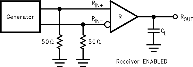
DSLVDS1048 10088803.pngFigure 15. Receiver Propagation Delay and Transition Time Test Circuit
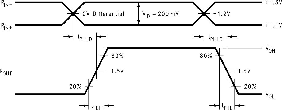
DSLVDS1048 10088804.pngFigure 16. Receiver Propagation Delay and Transition Time Waveforms
DSLVDS1048 10088805.png
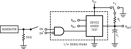
CL includes load and test jig capacitance.

S1 = VCC for tPZL and tPLZ measurements.

S1 = GND for tPZH and tPHZ measurements.
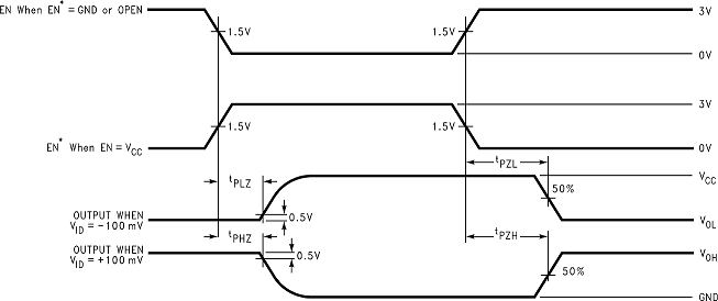
Figure 17. Receiver TRI-STATE Delay Test Circuit
DSLVDS1048 10088806.pngFigure 18. Receiver TRI-STATE Delay Waveforms