SNOSB66B August 2011 – November 2014 EMB1412
PRODUCTION DATA.
- 1 Features
- 2 Applications
- 3 Description
- 4 Revision History
- 5 Pin Configuration and Functions
- 6 Specifications
- 7 Detailed Description
- 8 Layout
- 9 Device and Documentation Support
- 10Mechanical, Packaging, and Orderable Information
パッケージ・オプション
メカニカル・データ(パッケージ|ピン)
- DGN|8
サーマルパッド・メカニカル・データ
- DGN|8
発注情報
5 Pin Configuration and Functions
VSSOP (DGN)
8 Pins
Top View
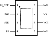
Pin Functions
| PIN | NAME | DESCRIPTION | APPLICATION INFORMATION |
|---|---|---|---|
| 1 | IN_REF | Ground reference for control inputs | Connect to power ground (VEE) for standard positive only output voltage swing. Connect to system logic ground when VEE is connected to a negative gate drive supply. |
| 2 | INB | Inverting input pin | TTL compatible thresholds. Connect to IN_REF when not used. |
| 3 | VEE | Power ground for driver outputs | Connect to either power ground or a negative gate drive supply for positive or negative voltage swing. |
| 4 | IN | Non-inverting input pin | TTL compatible thresholds. Pull up to VCC when not used. |
| 5, 8 | N/C | Not internally connected | |
| 6 | VCC | Positive Supply voltage input | Locally decouple to VEE. The decoupling capacitor should be located close to the chip. |
| 7 | OUT | Gate drive output | Capable of sourcing 3 A and sinking 7 A. Voltage swing of this output is from VEE to VCC. |
| - - - | Exposed Pad | Exposed Pad, underside of package | Internally bonded to the die substrate. Connect to VEE ground pin for low thermal impedance. |