JAJSE69 December 2017 HD3SS3412A
PRODUCTION DATA.
- 1 特長
- 2 アプリケーション
- 3 概要
- 4 改訂履歴
- 5 概要(続き)
- 6 Pin Configuration and Functions
- 7 Specifications
- 8 Parameter Measurement Information
- 9 Detailed Description
- 10Application and Implementation
- 11Power Supply Recommendations
- 12Layout
- 13デバイスおよびドキュメントのサポート
- 14メカニカル、パッケージ、および注文情報
パッケージ・オプション
メカニカル・データ(パッケージ|ピン)
- RUA|42
サーマルパッド・メカニカル・データ
- RUA|42
発注情報
9 Detailed Description
9.1 Overview
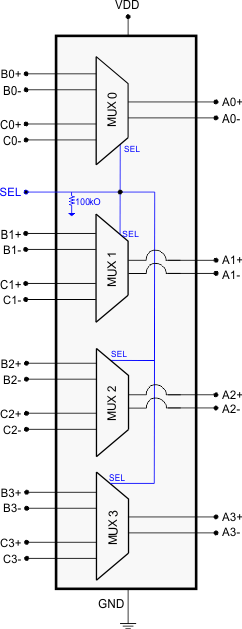
The HD3SS3412A is a high-speed passive switch offered in an industry standard 42-pin WQFN package available in a common footprint shared by several other vendors. The device is specified to operate from a single supply voltage of 3.3 V over the commercial temperature range of 0°C to 70°C. The HD3SS3412A is a generic 4-CH high-speed mux/demux type of switch that can be used for routing high-speed signals between two different locations on a circuit board. Although it was designed specifically to address PCI Express Gen III applications, the HD3SS3412A will also support several other high-speed data protocols with a differential amplitude of < 1800 mVpp and a common-mode voltage of < 2.0 V, as with USB 3.0 and DisplayPort 1.2. The device’s one select input (SEL) pin can easily be controlled by an available GPIO pin within a system or from a microcontroller.
9.2 Functional Block Diagram

9.3 Feature Description
The HD3SS3412A has a single control line (SEL Pin) which can be used to control the signal path between Port A and either Port B or Port C. The one select input (SEL) pin of the device can easily be controlled by an available GPIO pin within a system or from a microcontroller. The input signal is selected using the SEL pin.
Table 1. Mux Pin Connections(1)
| PORT A CHANNEL | PORT B OR PORT C CHANNEL CONNECTED TO PORT A CHANNEL |
|
|---|---|---|
| SEL = L | SEL = H | |
| A0+ | B0+ | C0+ |
| A0– | B0– | C0– |
| A1+ | B1+ | C1+ |
| A1– | B1– | C1– |
| A2+ | B2+ | C2+ |
| A2– | B2– | C2– |
| A3+ | B3+ | C3+ |
| A3– | B3– | C3– |
9.4 Device Functional Modes
Table 2 lists the functional modes for the HD3SS3412A.
Table 2. HD3SS3412A Control Logic
| CONTROL PIN (SEL) | PORT A TO PORT B CONNECTION STATUS | PORT A TO PORT C CONNECTION STATUS | ||
|---|---|---|---|---|
| L (Default State) | Connected | Disconnected | ||
| H | Disconnected | Connected | ||