JAJSE69 December 2017 HD3SS3412A
PRODUCTION DATA.
- 1 特長
- 2 アプリケーション
- 3 概要
- 4 改訂履歴
- 5 概要(続き)
- 6 Pin Configuration and Functions
- 7 Specifications
- 8 Parameter Measurement Information
- 9 Detailed Description
- 10Application and Implementation
- 11Power Supply Recommendations
- 12Layout
- 13デバイスおよびドキュメントのサポート
- 14メカニカル、パッケージ、および注文情報
パッケージ・オプション
メカニカル・データ(パッケージ|ピン)
- RUA|42
サーマルパッド・メカニカル・データ
- RUA|42
発注情報
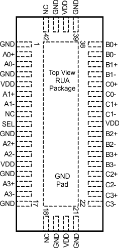
6 Pin Configuration and Functions
RUA Package
42-Pin WQFN
Top View

Pin Functions
| PIN | I/O | DESCRIPTION | |
|---|---|---|---|
| NAME | NO. | ||
| SWITCH PORT A | |||
| A0+ | 2 | I/O | Port A, Channel 0, High-Speed Positive Signal |
| A0– | 3 | I/O | Port A, Channel 0, High-Speed Negative Signal |
| A1+ | 6 | I/O | Port A, Channel 1, High-Speed Positive Signal |
| A1– | 7 | I/O | Port A, Channel 1, High-Speed Negative Signal |
| A2+ | 11 | I/O | Port A, Channel 2, High-Speed Positive Signal |
| A2– | 12 | I/O | Port A, Channel 2, High-Speed Negative Signal |
| A3+ | 15 | I/O | Port A, Channel 3, High-Speed Positive Signal |
| A3– | 16 | I/O | Port A, Channel 3, High-Speed Negative Signal |
| SWITCH PORT B | |||
| B0+ | 38 | I/O | Port B, Channel 0, High-Speed Positive Signal |
| B0– | 37 | I/O | lPort B, Channel 0, High-Speed Negative Signal |
| B1+ | 36 | I/O | Port B, Channel 1, High-Speed Positive Signal |
| B1– | 35 | I/O | Port B, Channel 1, High-Speed Negative Signal |
| B2+ | 29 | I/O | Port B, Channel 2, High-Speed Positive Signal |
| B2– | 28 | I/O | Port B, Channel 2, High-Speed Negative Signal |
| B3+ | 27 | I/O | Port B, Channel 3, High-Speed Positive Signal |
| B3– | 26 | I/O | Port B, Channel 3, High-Speed Negative Signal |
| SWITCH PORT C | |||
| C0+ | 34 | I/O | Port C, Channel 0, High-Speed Positive Signal |
| C0– | 33 | I/O | Port C, Channel 0, High-Speed Negative Signal |
| C1+ | 32 | I/O | Port C, Channel 1, High-Speed Positive Signal |
| C1– | 31 | I/O | Port C, Channel 1, High-Speed Negative Signal |
| C2+ | 25 | I/O | Port C, Channel 2, High-Speed Positive Signal |
| C2– | 24 | I/O | Port C, Channel 2, High-Speed Negative Signal |
| C3+ | 23 | I/O | Port C, Channel 3, High-Speed Positive Signal |
| C3– | 22 | I/O | Port C, Channel 3, High-Speed Negative Signal |
| CONTROL, SUPPLY, AND NO CONNECT | |||
| NC | 8 | — | Electrically not connected. May connect to VDD or GND, or leave unconnected. |
| 18 | |||
| 42 | |||
| GND | 1 | Supply | Negative power supply voltage |
| 4 | |||
| 10 | |||
| 14 | |||
| 17 | |||
| 19 | |||
| 21 | |||
| 39 | |||
| 41 | |||
| Center Pad | |||
| SEL | 9 | I | Select between port B or port C. Internally tied to GND through a 100-kΩ resistor |
| VDD | 5 | Supply | Positive power supply voltage |
| 13 | |||
| 20 | |||
| 30 | |||
| 40 | |||