JAJSJB2C June 2020 – June 2021 INA2290 , INA290 , INA4290
PRODUCTION DATA
- 1 特長
- 2 アプリケーション
- 3 概要
- 4 Revision History
- 5 Pin Configuration and Functions
- 6 Specifications
- 7 Detailed Description
- 8 Application and Implementation
- 9 Power Supply Recommendations
- 10Layout
- 11Device and Documentation Support
- 12Mechanical, Packaging, and Orderable Information
5 Pin Configuration and Functions
Figure 5-1 INA290: DCK Package5-Pin SC-70Top View
Table 5-1 Pin Functions: INA290 (Single
Channel)
| PIN | TYPE | DESCRIPTION | |
|---|---|---|---|
| NAME |
NO. |
||
| GND | 2 | Ground | Ground |
| IN– | 5 | Input | Connect to load side of shunt resistor. |
| IN+ | 4 | Input | Connect to supply side of shunt resistor. |
| OUT | 1 | Output | Output voltage |
| VS | 3 |
Power |
Power supply |
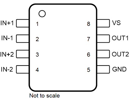
 Figure 5-2 INA2290: DGK Package8-Pin VSSOPTop View
Table 5-2 Pin Functions: INA2290 (Dual
Channel)
| PIN | TYPE | DESCRIPTION | |
|---|---|---|---|
| NAME |
NO. |
||
| GND | 5 | Ground | Ground |
| IN–1 | 2 | Input | Current-sense amplifier negative input for channel 1. Connect to load side of channel 1 sense resistor. |
| IN+1 | 1 | Input | Current-sense amplifier positive input for channel 1. Connect to bus-voltage side of channel 1 sense resistor. |
| IN–2 | 4 | Input | Current-sense amplifier negative input for channel 2. Connect to load side of channel 2 sense resistor. |
| IN+2 | 3 | Input | Current-sense amplifier positive input for channel 2. Connect to bus-voltage side of channel 2 sense resistor. |
| OUT1 | 7 | Output | Channel 1 output voltage |
| OUT2 | 6 | Output | Channel 2 output voltage |
| VS | 8 |
Power |
Power supply |
Thermal Pad can be left floating
or connected to GND.
Figure 5-3 INA4290: RGV Package16-Pin QFNTop ViewTable 5-3 Pin Functions: INA4290 (Quad
Channel)
| PIN | TYPE | DESCRIPTION | |
|---|---|---|---|
| NAME | NO. | ||
| GND | 6, 7 | Ground | Ground |
| IN–1 | 2 | Input | Current-sense amplifier negative input for channel 1. Connect to load side of channel-1 sense resistor. |
| IN+1 | 1 | Input | Current-sense amplifier positive input for channel 1. Connect to bus-voltage side of channel-1 sense resistor. |
| IN–2 | 4 | Input | Current-sense amplifier negative input for channel 2. Connect to load side of channel-2 sense resistor. |
| IN+2 | 3 | Input | Current-sense amplifier positive input for channel 2. Connect to bus-voltage side of channel-2 sense resistor. |
| IN–3 | 11 | Input | Current-sense amplifier negative input for channel 3. Connect to load side of channel-3 sense resistor. |
| IN+3 | 12 | Input | Current-sense amplifier positive input for channel 3. Connect to bus-voltage side of channel-3 sense resistor. |
| IN–4 | 9 | Input | Current-sense amplifier negative input for channel 4. Connect to load side of channel-4 sense resistor. |
| IN+4 | 10 | Input | Current-sense amplifier positive input for channel 4. Connect to bus-voltage side of channel-4 sense resistor. |
| OUT1 | 16 | Output | Channel 1 output voltage |
| OUT2 | 5 | Output | Channel 2 output voltage |
| OUT3 | 13 | Output | Channel 3 output voltage |
| OUT4 | 8 | Output | Channel 4 output voltage |
| VS | 14, 15 | Power | Power supply |